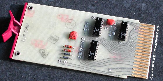
| Flip Chip Tester |
At that point Vince entered the "arena", and we exchanged some thoughts how to make the design more flexible, while sticking to the use of the Core and I/O Board. It was clear that we needed some form of I/O pins, but the requirement was that it must be possible to define each I/O pin separately to operate as an input or output.
 The FlipChip Tester must be easy to use.
That implies the requirement of separately controlable I/O pins.
The schematic shows how the I/O Board can be "upgraded" to meet that requirement.
SWITCH 1 is a switch that can be opened and closed under software control, and SWITCH 2
is a small (DIP) switch, which must be manually set to "open" or "close". CON 3 is connected to a contact
finger of the FlipChip you want to test, and CON 1 and CON 2 are available to implement
an other construction for the DIP switch, for example an external small switch, or 2 "mini-banana" sockets, very retro-stylish.
| contact finger | function |
|---|---|
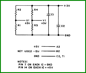
| A2 | +5V. power supply |
| B2 | -15V. power supply (if needed) |
| C2 | main Ground connection |
| T1 | Ground , or open |
The schematic diagram is needed for each contact finger of a FlipChip, and a FlipChip has 18 contact fingers at each
side of the module. That would mean that one single I/O Board would not be sufficient. However, all FlipChip modules
have the listed contact fingers common among them all.
As the contact finger B2 is always used for -15V power supply if the FlipChip needs it, the circuit
for this pin is only from "CON 1" to "SWITCH 2", and from "SWITCH 2"
to "CON 2" and the FlipChip contact finger.
The contact finger "T1" is neither connected to an input or output pin. Further, as the contact fingers
"A2" and "C2" are always used for power supply to the FlipChip, there is no need for a
connection to an input pin. However, "SWITCH 2" is useful to disconnect the contact finger. With the
omission of the pins B2 - T1 - A2 - C2 a single I/O Board is just enough to handle a single-height FlipChip.
To minimise external wiring, the Tester Board has all the components shown on a single printed circuit board.
"CON 1", "CON 2" and "CON 3" are pin headers, "SWITCH 2"
are DIP switches, and "SWITCH 1" are TTL buffers of which the output can be set into 3-state. The connections to
the I/O Board are positioned in such a way that the Tester Board can be mounted "piggy-back" on top of the I/O Board.

The diagram at the right shows an improved version of Rev.1 above.
This improved version one is called Rev.1a.
The only difference between Rev.1 and Rev.1a is the location of the SWITCH 2. The modification enables the use
of SWITCH 2 to disconnect the FlipChip contact finger completely.
Rev.1 only disconnects the contact finger to the output of the Tester hardware, the contact finger of The FlipChip is always
connected to the input of the Tester.
CON 1 and CON 2 are available to implement an other construction for the DIP switch.
| back to top |
We want to test a FlipChip, and not damage the FlipChip in the process of testing it ...
So, when the Tester is initially powered, all the SWITCH 1 switches are set in the "open" state by the software.
You must manually set the SWITCH 2 DIP switches for the contact fingers to the "open" position. With these precautions
you can safely connect a FlipChip to the Tester. Then you put the SWITCH 2 DIP switches for the contact fingers that
are an input of the logic of the FlipChip in the "closed" position. Likewise for the contact finger "C2" [GND].
To start the test of the FlipChip you close SWITCH 2 of the contact finger "A2".
That will apply the power supply to the FlipChip, and the software can start the test run.
When the test is completed (or aborted), you set the SWITCH 2 for the contact finger "A2"
back to the "open" position before you remove the FlipChip. When that switch is opened, all the SWITCH 1
switches are automatically put in the "open" state (hardware-wise). The software will also set all the
SWITCH 1 switches in the "open" state, but this is only done if you stop or abort the running test correctly.
Hence the hardware-wise option to revert to the safe state.
From this, it is clear that it makes sense to install a small switch via "CON 1" and "CON 2"
and set the DIP switch in the "open" position for the contact finger "A2" as this switch will be operated often.
| back to top |
| back to top |
The design is based on the use of the already available Core and I/O Boards. Several ideas were developed as the project progressed.
| Test Configuration | Core Board | I/O Board | Tester Board | Connector Board |
|---|---|---|---|---|
| single-height | 1 | 1 | 1 | 1 |
| double-height | 2 | 2 | ||
| quad-height | 4 | 4 | 2 | |
| hex-height | 6 | 6 | 3 |
So, if you have a test configuration for the single-height FlipChip, the upgrade for testing double-height FlipChips you requires one additional I/O Board and one additional Tester Board. The Connector Board is already suitable for single- and double-height FlipChips. The connector on the Connector Board is harvested from an old DIGITAL backplane.
| back to top |
The connections between the I/O Board and the Tester Board are straight-forward and 1-on-1. If the height of the components mounted on the I/O Board is below a certain value you can plug the Tester Board on top of the I/O Board. On the Tester board is one small connector to provide for some required interconnections between the Boards. From that small connector on the Tester Board one "air wire" goes to the I/O Board, and two "air wires" go to the Core Board. All 3 "air wires" are needed to implement the safety measurements as described.
Patch on the I/O Board
To meet the safety requirement that the connections to the FlipChip are not "hot" (not carrying signal voltages), a patch is
needed on the I/O Board. The pin #1 of all 74LS374 output latches on the I/O Board must be disconnected from Gnd.
If these ICs are in sockets, simply bend pin #1 135� ("up into the air"). If these ICs are soldered on the I/O Board, pin #1
is best cut off as close as possible to the I/O board, and then bend the pin 135�. Then, using a blank wire, connect all 8 pin #1's.
Use a suitable length of shrink isolation to prevent a short circuit between the wire and the components on the I/O Board.
The wire (pink in the picture) is connected to the pin "OC" of the small connector on the Tester Board.
The two "air wires" (green and blue in the picture) to the Core Board are only needed from the first Tester Board. The third "air wire" from the first Tester Board must be connected to all I/O Boards in the configuration, and the described patch must be applied to all I/O Boards in the configuration.

D:\Apps\RealConsole\FlipChip\software>flipchip -mm113data.txt

   FFFFF  LL    II  PPPPP      CCCC  HH  HH  II  PPPPP
   FF     LL    II  PP   P    CC     HH  HH  II  PP   P
   FFFF   LL    II  PPPPP     CC     HHHHHH  II  PPPPP
   FF     LL    II  PP        CC     HH  HH  II  PP
   FF     LLLLL II  PP         CCCC  HH  HH  II  PP

   ------------------ T E S T E R ------------v0.21---

[i]    setting the Tester in SAFE mode ...   succeeded.

______________________ Verify FlipChip in/out definition ______________________

  FlipChip id = M113, form factor - Single, logic family = TTL.

  side A2 : -  -  -  i  i  o  i  i  o  i  i  o  i  i  o  i  i  o   [sold. side]
            A  B  C  D  E  F  H  J  K  L  M  N  P  R  S  T  U  V
  side A1 : i  i  o  i  i  o  i  i  o  i  i  o  i  i  o  -  -  -   [comp. side]

[?]    is this M113 module definition correct [y/-] --> Y

[i]    setting the Tester in ACTIVE mode ...   succeeded.


[i]    Apply power to the FlipChip (switch ON row A finger A2)

   *** enter 'S' during the test to stop the running test
   *** enter 'T' to run the test for the M113 module  --> T

[i]    starting M113 FlipChip test

00001 P  11111111 11111111 11111111 11111111
00005 Q  11111111 11111111 11111111 11111111
00007 Q  11111111 11111111 11111111 11111111
00009 Q  11111111 11111111 11111111 11111111
00011 Q  11111111 11111111 11111111 11111111
00013 Q  11111111 11111111 11111111 11111111
00015 Q  11111111 11111111 11111111 11111111

   **** returned/expected data mismatch ***


   test terminated.

[i]    setting the Tester in SAFE mode ...   succeeded.

D:\Apps\RealConsole\FlipChip\software>
|
And here you see the content of the M113 testdata file, called m113data.txt, read by the PC Tester program.
M113
Single
TTL
*----------------------------------------------------------------------------
* this is a comment line and is not processed. The max length is 80 chars.
* The comment line can be used to add information about the module, for
* example the functional description of the module, power supply, etc., but
* also for separation of logical 'blocks', to add clarity.
*----------------------------------------------------------------------------
* Definition of the contact fingers.
*
*  pins on side-2 is the solder side
*  pins on side-1 is the component side
*
*  The definition line starts with a (upper/lowercase) 'D', followed by
*  a 2-letter combination indicating the contact finger side and row.
*  They can be "A1", "A2", "B1", or "B2".
*  "A1" and "A2" are mandatory, the single-height FlipChip fingers.
*  If the module is specified as being double-height ('DOUBLE' on 2nd line)
*  the "B1" and "B2" are also mandatory.
*  After the contact finger side and row letters follows 18 groups of
*  a space and a "value" which indicates the function of the contact finger.
*  possible "values" are:
*    i - FlipChip finger is an input
*    o - FlipChip finger is an output
*    n - FlipChip finger is not used, power supply or Test finger
*
* NOTE: all definition lines must be specified before the first Testvector.
*----------------------------------------------------------------------------
*   A B C D E F H J K L M N P R S T U V         (contact finger allocation)
dA2 n n n i i o i i o i i o i i o i i o
dA1 i i o i i o i i o i i o i i o n n n
*----------------------------------------------------------------------------
* Test vectors
*  _______ 1 ______ ______ 2 ______	NOTE: T1, A2, B2, C2 *not* in vector
*  ABCDEFHJKLMNPRSUVDEFHJKLMNPRSTUV
*                 --                    (P or Q template: '-' always '1')
*                 --                    (R template     : '-' don't care)
*
* Remark:
* the line counter in the generated output starts at the first Test line
*----------------------------------------------------------------------------
*  start test: set all inputs to a defined state
*
tP 111111111111111--111111111111111
*
*  fire test vectors and verify result with expected result
*
tQ 111111111111111--111111111111111
tR 111111111111111--111111111111111
tQ 111111111111111--111111111111111
tR 111111111111111--111111111111111
tQ 111111111111111--111111111111111
tR 111111111111111--111111111111111
tQ 111111111111111--111111111111111
tR 111111111111111--111111111111111
tQ 111111111111111--111111111111111
tR 111111111111111--111111111111111
tQ 111111111111111--111111111111111
tR 111110111111111--111111111111111
tQ 111111111111111--111111111111111
tP 111111111111111--111111111111111
* end of test data
|
As this is the test phase, I have not connected a FlipChip, so the expected data read back should all be logic "1". Because of
the "0" bit in the expected result (approximately at 3/4 of the test vectors), the Tester will report the data mismatch ...
When I connect a real FlipChip (like the M113), I must fill in the correct test vectors ! You can enter a minimum set of
test vectors, or a table of all possible input data with the expected output data. The minimum set for example for a 5-input
NAND would be INPUT="11111", expected OUTPUT="0". Then you cycle each input one by one, as in INPUT="01111", then INPUT="10111",
etc. where the expected OUTPUT is always "1". These test vectors can be hand-written and are good for a quick "GO / NO-GO" test,
but for a thorough test you must cycle through all input combinations ... which gets quickly a *lot* of test vectors!
Vince is working on a Perl script that accepts a logic definition and generates all possible input/expected output data ...
| back to top |
When all DIP switches are closed on the Tester Board, the following connections are made.
Example: testing the M113 (ten 2-input NAND gates).
 If you want to test a certain FlipChip for the first time (and nobody did it before you), you will have to start with looking up
the detailed information of the FlipChip in a DEC Handbook. You must know the used connections and its function. Then you must
write a small program that loads all possible input signal combinations and check their corresponding output results.
If you want to test a certain FlipChip for the first time (and nobody did it before you), you will have to start with looking up
the detailed information of the FlipChip in a DEC Handbook. You must know the used connections and its function. Then you must
write a small program that loads all possible input signal combinations and check their corresponding output results.
The software to test the FlipChip runs (for example) on a PC, but any computer with a serial port will work, so that old Mac or
SparcStation can be put to good use (as an old 386 ...).
Here is the diagram of the M113. This TTL module has ten 2-input NAND gates.
First, we put all DIP switches in the OPEN position. That is a good start, because if you overlook something you have a safe condition as the FlipChip is not connected to a driving output of the Tester. Check out the contact fingers of the FlipChip that are an output or not connected. For those contact fingers the corresponding DIP switches remain in the OPEN position to prevent accidental short circuits with the outputs of the Tester Board.
We put the DIP switches that correspond with the contact fingers of the FlipChip that connect to the inputs of the NAND gates
in the CLOSED position. Those DIP switches are the following.
A1 - B1 - D1 - E1 - H1 - J1 - L1 - M1 - P1 - R1 - S1 - D2 - E2 - H2 - J2 - L2 - M2 - P2 - R2 - T2 - U2.
Remark. It is no problem if the DIP switches that connect the Tester to contact fingers that are an output of the FlipChip are
set in the "closed" position, as the Tester will put the drivers in 3-state. It is just a precaution to avoid errors that might
cause damage to the MUT (Module Under Test).
Now that the DIP switches for the inputs and the outputs of the NAND gates are set to the correct position, you only must
check out the power supply connections. GND is connected to the contact fingers C2
and T1, so you put the DIP switch for those contact fingers on the CLOSED position.
As you started with all DIP switches in the OPEN position, the contact fingers B2, U1, and V1 are disconnected from the Tester's driving output.
The only DIP switch left is A2, the +5 Volt power supply. This DIP switch is used after the test program
is started, and the test program asks to apply the power to the FlipChip.
After you applied the +5 Volt to the FlipChip, you hit the "T" on the keyboard to start the test cycle.
From the procedure just described it is clear that you will often use the DIP switches.
It is wise to put the
DIP switch packages on sockets, or use the single-row headers to connect external (miniature) switches.
Also, as the FlipChip
that you want to test may have a short-circuit fault, it is wise to install the ICs of the Tester in sockets.
| back to top |

To keep the download time of this webpage low, you can see the testvector data file and the screenshot of the output after you click the link. Return to the website trhough the navigation section at the left or click the "Back" button in the browser. You can also right-click and select "Save as..." from the pop-up menu.
| back to top |
| back to top |