Part of a stepped microcode sequence on a "KM11 diagnostic paper" write down.
| Repairing a dead PDP-11/35 | KD11A |
How it all began ...
I have a PDP-11/35 in a BA11K box in my collection for a long time, but I never really tried whether it was in working condition.
As I had already moved it to 3 different locations, I thought it was about time to check out this box. So, moving approximately
50 kilos for the fourth time, but now to my test corner. First I opened the box by removing the top lid and made a note of all
slots and positions where boards were installed. Then I pulled all boards and put them safely in ESD bags. Cleaned the backplane
slots and removed dust from the inside. It was remarkable how clean this system was.
Moving on to the bottom. As long as the H742 power supply is at the rear side of the box this thing remains a really heavy beast.
Removed the bottom cover, and again I was looking at a very clean interior. There were no bent pins and all wiring looked fine.
So, time to connect mains power. I always use an 861 power controller on my desk. That way, I can turn on/off the system with the
front panel key, and disconnect mains power using the circuit breaker on the 861.
A first time "power on" is always a "moment of truth", but when I turned the key both fans started to run immediately and I did
not hear "additional" sounds which could be an indication of bad bearings in the fans. With my Fluke meter I measured all power
supply voltages of which +5V (logic) and +20V (core memory) are the most important ones. Of course, AC LO
and DC LO are also checked, and they looked fine as well. The +5V was slightly higher (5.25V), but as the
power supply was working under "no load" condition, this slightly higher output voltage can be expected.
All looking fine, and I switched power off. Being confident hat this system was in general in good shape, I installed all boards
in the backplane again. Normally, I would not do that, and start with a minimum configuration. When that configuration checks out
OK, I add a few boards until the whole system runs fine. In the case of the PDP-11/35, the minimum CPU consists of 5 boards, but
if the CPU has options installed, like floating point or memory management, you must install the options as well, because there
are jumpers on several basic CPU boards configuring the options. Especially the 11/35 (and 11/40) uses jumpers "all over the
place" to configure the processor options.
Anyway, I installed all boards and switched on power ... all fine! I tried to store some numbers in several memory locations, and
they read back all correctly. Now I toggled in the simple "chasing light" pattern program.
    address    data     instruction      comment
   ------------------------------------------------------------
    001000     012700   move #1,R0
    001002     000001
    001004     006100   rol R0
    001006     000005   reset            bus reset takes 70 ms
    001010     000775   br .-4           back to rol R0
|
Set the program counter to the start address and toggled START. The "chasing light" pattern was also running fine. So, now I connected a VT510 terminal to the console interface and used the switch register to DEP octal 65 in location 777564. A single "5" appeared on the screen. Hitting the "3" key on the keyboard and reading 777562 showed 63 octal on the DATA lamps. So, console connection is also working. Very happy, I switched off the 11/35.
A week later, I turned on the PDP-11/35. If the core memory would be OK, I should be able to simply load the start address and
toggle START. The "chasing light" program should run as core memory does not loose its last stored data.
And indeed, the "chasing light" program worked.
I installed the bottom and top cover and moved the box to another location. A few weeks later I switched on the PDP-11/35 again,
but now the "chasing light" program did not run, and worse, the front panel toggles increasingly responded more erratically, up
to the point that nothing worked any more. Not happy with this situation, I opened the top cover, but there was nothing "weird".
So, I placed the box on its side ... and I heard a sound ... opened the bottom lid and a long screw fell out. Apparently, one of
the long screws that mount a system unit (backplane) in the box was not tightened and moving the box "vibrated" the screw loose.
The distance between the bottom cover and the pins of the backplane is just a few millimeters, so this screw had caused a short
circuit condition to some of the logic of the processor. This fault would not go away "from itself". If I wanted to get this
11/35 back in working condition, I had to find the one or more damaged ICs.
Back to the test bench. After removing the top and bottom cover, I first checked the power supply voltages. They were all fine, so at least the damage was not "major", like many ICs fried because of a way too high supply voltage. The +20V for the core memory is only connected to the core system backplanes, thus the short circuit could not have connected +20V to the CPU logic.
So, what is the system doing? Maybe there is a pattern, possibly leading to some solution.
Before switching on power, I set the switch register to 000077, and the ENA/HALT switch to
HALT. When the 11/35 is switched on, the ADRS lamps are all off and the
DATA lamps have some value, but is never the same when the system is switched on. BUS
and CONS are also always on. When I set the switch register to any value and then toggle
LOAD ADRS, the ADRS lamps remain all off (they should show the switch setting of the
switch register), and the DATA lamps all go on. That's wrong as well. Further, RUN,
PROC, BUS, and CONS go on. After that, the front panel is
completely not responsive. While the ENA/HALT switch is in the HALT position,
toggling START (initialize, "reset") has no effect either.
Needless to say, you need documentation to debug this system. From bitsavers /pdf/dec/pdp11/1140 you can download the PDP-11/35 (/40) documentation. There are several documents, and it does not harm to read them all, but the manuals that you really need are
| Back to top |
The 11/35 is an overwhelming piece of hardware. The basic processor consists of 5 boards, 4 "hex width" and one "quad width" board. That brings the count of ICs to almost 500! This 11/35 also has the memory management option, which adds another 100 ICs, and more complexity ... and one or maybe more are defective. So, where to begin? I can only describe how I went along. Maybe that was not the best approach, but it learned me a lot of the PDP-11/35 and I did things I had not done before - it is an experience of which much was learned.
After reading, I figured that it would be very useful to have a KM11 diagnostic panel. I do have an original KM11, but from
previous use (to check a dead PDP-11/10, but that's another story), I know that several bulbs are dead. So, the displayed
microcode bits are not correct. I decided that after some 7 years (!) it was time to build the KM11 replica kit designed by Guy
Sotomayor. You can put the KM11 diagnostic panel on an "extender" in slot 1 position E or position F. When the KM11 is in
position F you can execute the 11/35 microcode stepping and see relevant signals on the 28 LEDs. When the KM11 is installed in
position E you can see information of the floating point and memory management module. A first "quick check" showed that the
processor is actually executing the microcode, so the CPU is not completely "dead".
What I also learned is that you really need to have the documentation available. I made copies of what seemed to me the
most relevant pages at this point. I can make notes on the copies and keep the original documentation in "virgin" condition.
I never tried microcode stepping before, so this was a new learning moment for me. Reading the LEDs of the KM11 was a
time-consuming task and then writing it down, every microcode step again. I have drawn a small table with the KD11-A mask layout
for the KM11 and duplicated that 25 times on a single A4 sheet of paper. This way, I can step the microcode, put a cross on the
sheet for each lamp that is lit and continue. Afterwards, at home, I can decode the patterns, look up which microcode mnemonic
each pattern represents and check the logic flow. (It is just 11 degrees Celsius at the moment in my "museum").
| Not knowing where to start, I figured looking at the executed microcode steps might give me clues as what the processor is doing. After switching power on I stepped through the microcode, marking down the lit "lamps" on the "KM11 diagnostic paper". The results are at the right side. PUPP is the abbreviation for "Previous Microcode Program pointer" and BUPP is the abbreviation for "Base Microcode Program pointer". In the KD11-A documentation and schematic diagrams the word "microcode" is abbreviated to the single letter "U". Reading the crossed lamps of the "KM11 diagnostic paper" and writing the value down in octal, I came to this table. Each new line is the result of "toggling" the MCLK switch down and up again on the KM11. Using the microcode listing (see page 37, KD11-A Field Maintenance Print Set), I can add the microcode mnemonics. It is clear that the microcode is executing a loop. |
     PUPP  BUPP   mnemonic
    -----------------------
      030   315
      315   046    CON06
      046   026    CON04
      026   046    CON06
      046   026    CON04
      026   046    CON06
      046   026    CON04
|
|
Searching the microcode flow diagrams (pages 12-19, KD11-A Field Maintenance Print Set), I found the executed microcode sequence
on page 16. The loop tests for a switch from the front panel. So, to fall through this loop I have to toggle one of the switches.
LOAD ADRS is an obvious choice ... I toggled LOAD ADRS and clocked MCLK
several times. The result is at the right side. The "CON06 - CON04" loop is exited with CON07. After a few more microcode steps the processor is back in the "CON06 - CON04" loop. Further nothing has changed. To get more insight on what is happening, I read chapter 4 of the KD11-A processor maintenance manual. Very enlightening! Looking at the microcode flow diagram (page 16 FMPS), the microcode LAD00 should have been executed after CON11, but instead CON05 and CON13 are executed. At the right side of page 16 you can see that the microcodes CON05 and CON13 are executed after power up. It seems that the microcode to process the LOAD ADRS toggle is never executed. |
     PUPP  BUPP   mnemonic
    -----------------------
      026   046    CON06
      046   026    CON04
      026   027    CON07
      027   044    CON08
      044   047    CON09
      047   045    CON10
      045   050    CON11
      050   030    CON05
      030   315    CON13
      315   046    CON06
      046   026    CON04
      026   046    CON06
      046   026    CON04
|
Some initial conclusions
On page 16 FMPS is a branch after the microcode CON06 and is tagged SWITCH. The "leg"
-SWITCH is taken if no toggle has been pressed, and that is where the processor loops waiting for an
activated toggle from the front panel. This signal SWITCH can be found in the schematic diagram on page 61
FMPS, the output of the 7474 flipflop E12 pin 8. As the microcode flow executes as expected at this point, I can assume that the
"famous" 7474 flipflop is working. Looking at the signals, you see that LOAD ADRS, CONT,
EXAM, and DEP can trigger the flipflop via the 7430 E9.
|
Further, gates E5, E6, E7, E8, and E23 generate the signals BUBC0(BUT30), BUBC1(BUT30),
and BUBC2(BUT30). I get back to these signals further down ... These 3 signals form a binary code unique for
the pressed toggle switch, see the table at the left. I measured these signals with the Fluke Voltmeter.
At microcode CON10 it is checked which toggle has been activated. The BUT code is 30. BUT stands for "Basic Microcode Test". At microcode CON11 the test changes the BUT code 30 to 37, 35, 36, 34, or 32 depending on the activated toggle switch. Note that the low 3-bit code matches the code in the table! At the bottom of the microcode flow diagram on page 16 FMPS, you see the decision "twisties" for the activated toggle switch and each branch continues on page 17. |
But, unfortunately, whatever toggle switch is pressed, the BUT code does not change. As a result, the "twisty" for code 30 "CONSOLE RECYCLE" is executed. So, the activated toggle is not "seen". The "good" news is that while stepping through the microcode the ADDRESS and DATA lights on the front panel light on and off. So, more of the processor hardware is OK. The question is "how (where) is the microcode changed?"
To understand more of the power-up sequence of the processor, I had set the switch register to 000077, and this time the
HALT/ENA switch to ENABLE. After switching on, the ADDRESS
lamps on the console are all off and the DATA lamps show 162700 this time.
The executed microcode sequence is now 337 - 334 - 335 - 332 - 333 - 002. This sequence is described on page 11 FMPS.
Depending on the position of the HALT/ENA switch, the branch to SERVICE D or
CONSOLE A is taken. Could it be that SERVICE D on page 11 is a typo?
I find microcode 002 on page 15 top left, but it is then name SERVICE B. The sequence continues
015 - 010 - 216 - 215 - 115 - 326. This looks like the TRAP A flow on page 11, to label
-MM FAULT, and then continuing in the flow of TRAP D: 327 - 113 - 330 -
331 - 077 - 140 - 332 - 333.
And then we are back at the decision HALT/ENA switch on ENABLE or on
HALT. During these sequences the signal MSYN is also pulsed, so again, more
hardware seems to be fine.
But how are the Base Microcode Test (BUT) low 3 bits changed?
On page 17 FMPS you can see the loop that is executed for the front panel toggle switches. CON04 tests
whether a toggle switch is active. For a detailed inspection you use the microcode of CON04 (026) and
look at page 37 FMPS. That table lists of each of the 256 microcodes the state of all 56 bits of the microcode instruction.
The bits that are relevant at this point are the UBF bits. UBF stands for
Microcode Branch Field. With these bits the multiplexers are controlled which modify the BUT value
(Basic Microcode Test), see page 42 FMPS at the lower left side.
The SWITCH signal (from page 61 FMPS) is connected to multiplexer E97, input D6. The
UBF bits for microcode CON04 is 06. If the UBF bits are 06,
then the output of multiplexer E97 equals the state of the signal SWITCH.
Back to page 16 FMPS. Microcodes CON06 and CON07 test whether the signal
SWITCH is active. (Why CON06? Read the maintenance manual ...). As the flow
continues to CON07, we can conclude that E97 is OK (at least, input D6 appears at the output and this
signal reaches the correct destination).
Microcodes CON08 and CON09 form a switch debounce loop. I assume that when you step through the microcode the delay loop time is expired, and thus microcode CON10 is reached. All this confirms my understanding and the link between the microcode flow diagrams and the schematic diagrams.
Microcode CON10 checks which toggle switch was activated. Note that next to the rectangle that
describes CON10 the number "030" is written. That is the Basic Microcode Test number. As described earlier,
the toggle witches are not "seen" and microcode CON05 is executed. The value of microcode
CON05 is "030".
The value of microcode CON10 is "045". Back to page 37 FMPS. Microcode CON10 sets the
UBF bits to 30 (octal). Back to page 42 FMPS. UBF bits set to 30, thus the signals
UBF0, UBF1, UBF2 are "0" and UBF3,
UBF4 are "1". These 5 signals are used to enable the 3 multiplexers and connect a specific input to the
output. To be exact, E72 en E81 are enabled en connect input D8 to the output, E98 en E90 are also enabled, and here relevant,
of multiplexer E98 the input D0 appears at the output.
The output of E81 generates signal BUBC0.
The output of E72 generates signal BUBC1.
The output of E98 generates signal BUBC2.
The output of E90 generates signal BUBC3.
The output of E82 generates signal BUBC4 and BUBC5.
The BUT code 030 is the "base code" which can be modified by the executed test (result). I have not
checked, but I guess that the BUBCx signals are all wired-OR signals. As soon as one of the connections
of a wired-OR becomes active, the combined signal becomes active. Thus, by switching an input of the multiplexer to the output
(based on the UBF bits), the next to be executed microcode instruction is determined. Let's see if this
is correct for UBF bits equal to "030".
BUBC0 = E81/D8 = K5-6 BUBC0(BUT30)
BUBC1 = E72/D8 = K5-6 BUBC1(BUT30)
BUBC2 = E98/D0 = K5-6 BUBC2(BUT30)
These signals all come from page K5-6, that is page 61 FMPS, top right side! Checking the logic circuits you can see that
BUBC0(BUT30) = EXAM + LOAD
BUBC1(BUT30) = CONT + LOAD + START
BUBC2(BUT30) = EXAM + CONT + LOAD +
DEP
and the table of the front panel toggle switches matches.
If we add the octal value of the activated toggle switch to the Base Microcode Test number (030), we get the microcode numbers
for LOAD ADRS, EXAM, CONT, DEP,
START, and CONSOLE RECYCLE (page 16-17 FMPS).
I measured the output signal of the gates E8, E7, E23 en E12 (page 61 FMPS), and they are fine. The signal SWITCH, output E12, is also OK. So, continuing on page 42 FMPS. The signals BUBCx remain "0" as the BUT remains "030". But I measured that the gate output signals arrive on the inputs of the multiplexers and that the UBF bits are as expected. So, could it be that the multiplexers are defective? But it would be a weird coincidence that all 3 are defective, although all signals are tied to pins on the backplane ...
New idea
The combined signal SWITCH is latched by a 7474 flipflop, but the signals of the front panel toggle switches
are _not_ latched. As far as I know, in my tests, I stepped the microcode, toggled the LOAD ADRS toggle switch
and continued stepping, seeing the (incorrect) result. However, as the toggle switch signals are not latched, at the moment they are
evaluated their signals are no longer active!
|
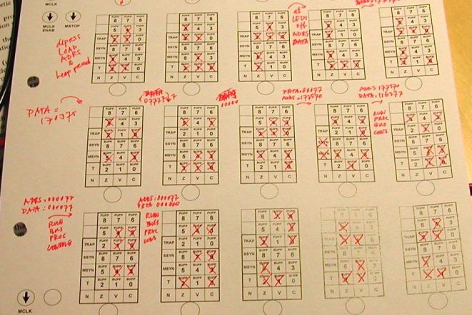
At the right side you can see the microcode execution when the LOAD ADRS toggle switch is pressed and
kept pressed while the following microcode instructions are stepped. After CON11, the microcode 030 is
now changed to 037, LAD00! The microcode instructions that follow are exactly matching the flow diagram on page 17 FMPS.
What is also striking, is that after execution of LAD01 the front panel DATA lamps
show 000077, the setting of the switch register. After the execution of LAD03 the front panel
DATA lamps still show 000077, but now the ADDRESS lamps also show 000077. You can see
this sequence in the picture "KM11 diagnostic paper" above. I repeated this test with the EXAM toggle switch. If the toggle switch is not kept pressed, but only momentarily, the BUT code remains 030. When the EXAM toggle switch is kept pressed, the BUT code changes to 035, and the next microcode instruction executed is 053 (EXM01). And the complete microcode instruction flow for EXAM is correctly executed as described on page 17 FMPS. |
     PUPP  BUPP   mnemonic
    -----------------------
       :     :
      046   027    CON07
      027   044    CON08
      044   047    CON09
      047   045    CON10
      045   050    CON11
      050   037    LAD00
      037   051    LAD01
      051   052    LAD02
      052   033    LAD03
      033   030    CON09
      030   315
      315   046
      046   026
|
Although I had already read most of the KD11-A processor maintenance manual, I only vaguely remembered that you can do something
with the microcode address and the console Switch Register. Reading that part again gave me a new idea to test the console
switches. Till now I used the switches "MCLK" and "MCLK ENAB" of the KM11 diagnostic
panel to step through the microcode. However, there is a comparator that compares the 8-bit microcode address "PUPP"
with the 8 lower Switch Register switches. When the microcode address matches the 8 Switch Register switches, the signal
"UPP MATCH H" is activated. If the "MSTOP" switch of the KM11 diagnostic panel is active
and the signal "UPP MATCH H" becomes active, the execution is halted. My next tests will be the following.
When I step through the console switch microcode loop while holding the LOAD ADRS toggle pressed, the CPU
will execute that path. When the microcode execution of LAD00 is done and I let the CPU run "full speed", the
console becomes unresponsive. Unfortunately, I do not know what is executing (if there is any execution at all).
. . . to be continued . . .
| Back to top |