| Real PC05 for SIMH via a PC |
|
Edward wanted to add a real peripheral device to his "blinkenlight" *real* PDP-11/70 console based on the Core and I/O board that
I developed back in 2003 or something like that. Nowadays (2017) we have Oscar's PiDP-8 and PiDP-11/70 which both use a
Raspberry Pi to run SIMH *and* interface the front panel switches and lights. Edward has a PC05 papertape reader/punch which
he wants to connect to his simulated PDP-11/70, and he asked me whether I could make an interface that at one side simply
connects to the PC05 and at the other side connects to the PC using an RS-232 connection or a USB connection. On the PC runs
either Windows 10 or Linux.
One design decision was immediately made: no USB! USB code is complex and not trivial. Standard RS-232 is a lot easier to
implement. If you want USB, my advice is "do not develop a USB connection yourself, but use a serial port". I know that
libraries are available for the USB stack, but you also need driver software in the PC to make a successful connection.
To have a USB connection, buy an FTDI "USB to serial" connection cable ($20). FTDI supplies drivers for most operating systems,
so that issue is solved. No time to waste on a USB stack etc. The "serial" side of the cable has many variations in the
physical connection (plug, header) and logic levels (5V, 3.3V). The only catch is that you must make sure that you buy an
original cable from FTDI, no a cheap China copy. The FTDI drivers do not work with the "China stuff".
Time to read the PC04/PC05 documentation and study the schematics. I found out that I should be happy that he has a PC05,
and not a PC04. The PC04 is intended for the PDP-8 (and PDP-12, PDP-15) computers, the PC05 is intended for the PDP-11.
Although the units look very similar on the outside (minus one push button), the control hardware is very different inside.
In the PC05 all the control logic is inside the unit, whereas the PC04 only has the drive hardware for the reader stepper motor
and the hardware for the puncher. Most of the controlling hardware (FlipChip modules) is located inside the PDP-8! That makes
the PC05 a lot easier to interface, because most of the "smart stuff" to control the reader and puncher is in the PC05.
The PC05 uses 2 flatcables to connect to the PC11 controller (M7810) in the PDP-11 computer. Just as the reader section and the punch section inside the PC05 are two separate devices, so is the interface connection. One flatcable is for the reader, the other flatcable is for the punch.
I started on the reader interface, and as far as I can see the following interface signals are available. I used the schematic PC05-0-4 Rev. K "CONTROL AND POWER SCHEMATIC (READER)" from bitsavers.
              RSF=     6011      / Reader Skip if Flag
                                 / If the reader flag is set, it indicates that a character
                                 / from the tape is available, the next instruction is skipped.
              RRB=     6012      / Read Reader Buffer
                                 / The reader character buffer is OR-ed with the accumulator.
                                 / By clearing the accumulator before RRB, the accumulator
                                 / will hold the character read from the tape.
                                 / The instruction also clears the flag.
              RFC=     6014      / Reader Flag Clear
                                 / Clear the reader flag *and* initiate the reading of the
                                 / next character from tape. The reader flag will be set by
                                 / the completion of the read operation.

     / initialize the reader
     / As the reader skip flag is cleared at power-up and a reset, the flag must be set
     / somehow to indicate that the reader has "received" the first character.
     / This is accomplished by simply "reading" the first "character" *without* checking
     / whether the reader skip flag is set.

              RFC

     PTRIN,   .-.                / read papertape frame into [AC]
     RDRLP,   RSF                / await input ready
              JMP      RDRLP
              CLA
              RRB RFC            / read character
              JMP I    PTRIN
|
It is common in PDP8 programs that they define the IOT instructions that are used. The program code also explains what the
SKIP output signal from the reader is used for. An other typical PDP8 assembler usage is the
"combination" of bits of the OPR instructions and likewise for bits of the IOT instructions, if possible. Here you see the
example of combining the RRB and the RFC instruction. Effectively the assmbler
will generate *one* instruction, which is the OR of the two given instructions. Thus, the IOP2 pulse and IOP4 pulse are
combined in one instruction (and the hardware will take care that the two pulses are executed one after the other).
All that is needed for the interface is that it mimics the behavior of this program loop!
The translation from the PDP8 software papertape reading routine to interface firmware is as follows.
The punch interface is completely separated from the reader interface.
              PSF=     6021      / Punch Skip if Flag
                                 / If the punch flag is set, it indicates that a character
                                 / punch cycle is completed, the next instruction is skipped.
              PCF=     6022      / Punch Clear Flag
                                 / The punch flag is reset.
              PPC=     6024      / Punch Put Character
                                 / The low 8 bits of the accumulator are copied to the punch
                                 / buffer, starting the output.
              PLS=     6026      / Punch Load Sequence
                                 / This instruction is an OR of PCF and PPC. The output is
                                 / started and the punch flag is reset. The PC05 hardware
                                 / executes this in separate steps.

     / initialize the punch for output
     / As the punch flag is cleared at power-up and a reset, the flag must be set somehow
     / to indicate that the punch is ready to receive a character to be punched.
     / This is accomplished by simply punching a NULL character *without* checking whether
     / the punch is ready to receive that character. NULLs are expected to be leader of tape.

              CLA
              PPC                / output a NULL (blank tape, no holes)

     PTPOUT   .-.                / write [AC] to papertape punch
     PCHLP,   PSF                / await till puncher ready
              JMP      PCHLP
              PLS                / write character
              JMP I    PTPOUT
|
In this example the PCF and PPC instructions are combined. As this combination is
so common, a "new" mnemonic is defined, PLS.
Again, all that is needed for the interface solution is that it mimics the behavior of this program loop!
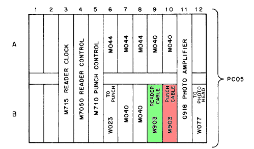
The reader and punch are connected using 2 "paddle" boards, one for the reader and one for the punch. When you look at the backplane at the side where the modules are plugged in, the reader is connected in slot #9 position "B", and the punch is connected in slot #10 position "B". Note that the PC05 "MODULE UTILIZATION LIST" shows the allocation from the rear side, that is the wire wrap side! Looking at the front side (where the modules are plugged in), slot #1 is at the right side, position "A" is the upper row and position "B" is the lower row. Thus, slot #1 and slot #2 at the right side are not used.
| pin | READER (slot #9) | PUNCH (slot #10) |
pin "number" allocation |
|---|---|---|---|
| B1 | RDR RUN* | INITIALIZE* |
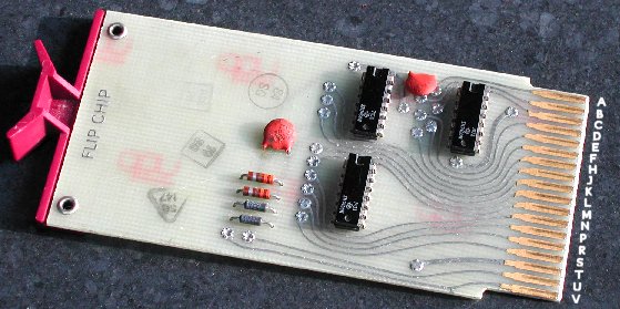 (this is an "M113" FlipChip module, but the contact fingers are the same) The contact finger "A1" is at the component side (left top), and "A2" is on the solder side, behind "A1". Single-sided modules often omit the "2" in the contact finger name, and refer to the contact fingers as "A", "B", etc. If no side is specified, the contact finger is on the solder side. The figure shows the location of the contact fingers when you look at the component side. |
| C1 | GND | GND | |
| D1 | INITIALIZE* | OOT | |
| E1 | INT* | INT | |
| H1 | OOT | ACTIVE* | |
| J1 | SKIP* | SKIP | |
| L1 | INITIALIZE | RDR FEED | |
| M1 | DATA0 | DATA0 | |
| P1 | DATA1 | DATA1 | |
| S1 | DATA2 | DATA2 | |
| D2 | IOP1 | IOP1 | |
| E2 | QUALIFY | QUALIFY | |
| H2 | IOP4 | IOP4 | |
| K2 | IOP2 | IOP2 | |
| M2 | DATA7 | DATA7 | |
| P2 | DATA6 | DATA6 | |
| S2 | DATA5 | DATA5 | |
| T2 | DATA4 | DATA4 | |
| V2 | DATA3 | DATA3 |
EK-PC11-TM-003, "PC11 high-speed reader/punch and control manual" lists in Appendix A the correlation between the signal names
used in the schematic diagrams of the PC04/PC05 and the names used in the PC11 documentation. What is interesting to see, is
that the PC11 does not use the IOP1 of the reader, nor the IOP1 and
IOP2 of the punch!
 |
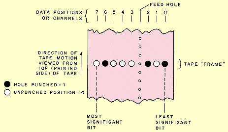 |
To make sure to get the databits connected correctly, here is a small piece of paper tape. As you can see, there are 5 columns, then the (smaller) feed hole, and then 3 more columns. The right-most hole of the 3 column part is bit 0. The left-most hole of 5 column part is bit 7.
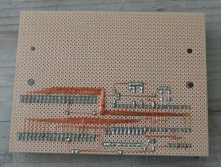
The PC05 interface is built on a piece of "experiment perforated board". The connections are soldered using enamel lacquered
wire (0.3 mm). With a hot soldering iron you can burn off the isolation and obtain a nice tinned wire end ready to be soldered
to the pin of an IC (socket) or resistor. Make sure you do not inhale the fumes or get fumes in your eyes ...
 |
 |
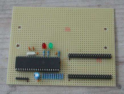
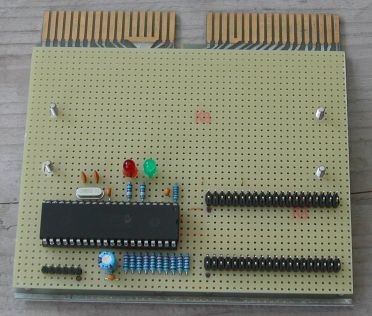
As you can see, only the 18F4550 PIC is needed plus a few "standard" components, like the 20 MHz crystal for the PIC, a few
capacitors and several pull-up resistors. The pull-up resistors are needed, because the 8 reader data outputs are open collector.
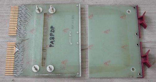
Two 2x20 pin headers connect two flatcables. The other end of the flatcables connect to "paddle boards" that can be plugged into
the backplane of the PC05. The "READER" paddle board goes into slot B09, the "PUNCH" paddle board goes into slot B10. A 6-pin
header connects RxDATA, TxDATA, GND and +5V to the USB to TTL cable. RTS*, CTS* and DSR are not used.
 |
 |
The "experiment perforated board" is mounted on an M9202 UNIBUS system unit interconnect bridge with 10 mm
standoffs. The M9202 consists of two long cards that go into the last slot position A-B of one system unit (backplane) and the
first slot position A-B of the next system unit. Between the two boards is 2 feet of "UNIBUS" flatcable.
The two boards are separated and the interconnection flatcable is removed. Finally, the top part with the handle is cut off.
What remains is a board that fits perfectly in the empty slot 2 of the PC05 backplane.
The only connections to the PC05 is one power cable (115V AC) and one USB data cable to the PC.