Spin off : PDP-8/e for the RealConsole
This page is written in a chronological sequence, as the project evolved. That means that a finished job, for example
the mechanical construction of the pdp8/e simulator, is not a complete chapter but consists of several snippets
scattered "all over the place". I have put here some links inside this page to collect all scribbling about a subject.
If you want to print this page on A4 or Letter format, set the scaling in the printer driver to 80%.
| Quick jumps within this page |
|---|
|
|
|
Introduction
While I was working on the change of the Core Board replacing the 6802 micro-processor for the more ready available
6809 CPU I also needed a modified monitor (debug) program. I started with re-writing my 6802-based
monitor, and started a search for a 6809 assembler .... and found the website of Alan R. Baldwin
ASxxxx Cross Assembler (for 6809).
In the assembler package was a 6809-based monitor!
I decided that it would be stupid to re-invent the 'wheel'
and implemented the "MONDEB-09" monitor.
After the monitor worked on the Core Board I made a few changes and
put in some additions, among which the RealConsole firmware, the Tiny BASIC program (found in comp.sys.m6809 written
by John Byrns), and a 6809 disassembler (first appeared in Byte, Feb. [1982], written by J. Dubner and then modified
by P. A. Vazquez [1988]).
I renamed the resulting monitor "CORESYS".
Browsing the Internet I also stumbled upon the FLEX User Group website
Flex User Group File Exchange.
The page shows a link to a ZIP file called "tcj_sub" by Frank Wilson. Inside that ZIP file is a 6809-assembler
written simulator for the PDP-8/e ... my thought was: "wouldn't it be nice to run a PDP-8 on *only* the
Core Board with a (replica) PDP-8/e console connected to it through the I/O Board" ?!
If you wonder "what's a PDP-8 ?", check out
Doug Jones's DEC PDP-8 Index as a
starting point for some good reading.
Falling and getting up again (several times)
One thing lead to an other, and before I knew it I was buried into making adjustments to the source code to port
the code to the RealConsole hardware, the Core Board.
After a few days of study I started to change the code to get it running on the Core Board hardware. That took a few
weeks with varying success. It worked, but then I applied too many changes in one update and the simulator did
not work as it should anymore. Reverting to an old version and applying the 'fixes' one by one, I finally found
a stupid typo! I received from Vince a few small test programs to load with the binary loader of the simulator:
- interrupt-based input and output
- interrupt-based input and print "HELLO"
- a check for existence of the timeshare option
The Core Board's serial port is connected to my PC.
On the PC, I run the program Hyperterm, with the following
settings: 9600 Bd, 8 data bits, 2 stop bits, no parity, no flow control. Since the emulator does not support the
various modem protocols from Hyperterm, the "Send Text File..." option is used.
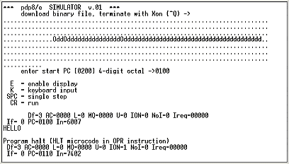
The small programs all loaded fine, and worked. As the simulator used a default PC 0o0200 (of the PDP-8), I added
the prompt that asks what the PC value must be at start. The timeshare test does *not* print "SORRY",
but prints "OK"! Next I tried to load FOCAL69, but the BIN loader choked.
To get a grip of what was going on I changed the polled-I/O routine to interrupt-driven with a circular buffer to
store the received data. That allowed me to do some printing while the file download was in progress. The print out
shows what kind of data is received, Leader, Origin or Field specification, Data or Trailer.
It got me puzzled for a few days why FOCAL69 failed to load, but finally I found the problem.
It was not in the simulator 6809 code, but Hyperterm! Here is a small part of the binary dump I made to find the problem.
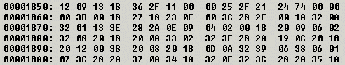
Every 2 bytes are transformed into a 12-bit PDP-8 word. The byte at offset 0x185D (74) and the next byte form a new
Origin specification. At the offset 1898 the FOCAL69 file contains a data byte sequence 0D - 0A.
The "0D" is the 2nd byte of a 12-bit word, and the "0A" is the first byte of the next 12-bit word. Hyperterm
interprets the sequence as CR/LF, and does not send the LF! All subsequent
data is shifted one byte and that will eventually lead to a bad data value, as the next Origin specification (bit 6 set)
in the file is interpreted as data and that can not have bit 6 set, so the BIN loader aborts with an error.
I could not find a way to make Hyperterm send *all* bytes. The work-around is to use the good old DOS prompt!
First you "Disconnect" Hyperterm. Then you type at the DOS prompt "type FOCAL69.BIN > com1:"
the file is sent to the Core Board.
After the DOS prompt re-appears, you click "wait for Call" in Hyperterm
and enter ^Q (control-Q).
That signals that the download is finished. I've got FOCAL69, FOCAL71, and
ODT working at this moment.
In the process I added screen output control (VT100 escape sequences) and added ASCII "artwork" to
display the state of the simulated PDP-8/e. Single stepping the PDP-8 instructions and have a display of the registers
is nice, but the performance penalty is *huge* (though nice to watch for a few minutes). I removed the "VT100" code,
but added a few command line options to show the requested PDP-8 register; it is not 'real-time' updated on the screen
anymore.
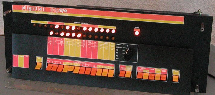
Making a replica of the PDP-8/e console - step 1
Of course, you would not rip the console from a real PDP-8! So you must make one yourself!
Here is a description of how I did it, but let me start to say that the final result depends very much on how
accurate you work with metal or whatever material you use, how much time you spend on it, and the availability
of good tools. Patience is your best friend!
The first step is finding suitable switches. The PDP-8/i uses different switches than the PDP-8/e. The PDP-8/i shows
all registers and its state in lights *at the same* (lots of 'blinkenlights'!), but the /i console has switches which
are difficult to find, especially if you want to make your replica console a little smaller than the real console.
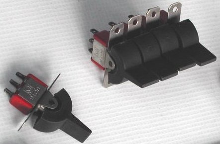 The switches of the 8/e (with a lever) are available at the better electronic DIY shops, but the 8/e uses a so-called
"Indicator Selector Switch" which determines the register displayed on the 12 lights.
The switches of the 8/e (with a lever) are available at the better electronic DIY shops, but the 8/e uses a so-called
"Indicator Selector Switch" which determines the register displayed on the 12 lights.
So there are fewer lights on
the PDP-8/e, thus less blinkenlights. The advantage is less work in wiring the console and one single I/O Board
is all it takes to interface to the PDP-8/e console ... you'd need *two* I/O Boards to connect a PDP-8/i console!
Wait a minute, the switches are black!"
Yep, the switches and keys (momentary switches) must be painted to the yellowish and sort of orange color just like
the original PDP-8/e. I used the following procedure.
- Use degreaser to remove grease and fingerprint oil from the black plastic lever.
- Use fine sandpaper to form a better grip on the surface of the lever for the paint.
- Use degreaser to remove new fingerprints and the dust from the lever.
- Put all switches and keys that must be painted in one color next to eachother with two inches between each.
- Spray with a spray can plastic primer on all sides of the levers.
- Wait 10 to 15 minutes. If you wait longer the primer looses its adhesive features for the ...
- Spray with a spray can the desired color. Do *not* try to cover the black lever in one go with the
yellowish (or orange) color. Much better is painting the levers in 4 or 5 times with thin layers. Let each layer
dry for at least 10 minutes; this depends on the paint you use. I used an acrylic lacquer because it is fast drying,
has a hard finish, and it is light resistant.
The colors I used are RAL2000 (sort of orange) and RAL1028 (yellowish).
Though the real PDP-8/e I ever saw was Pete's [Turnbull] many moons ago, guessing from the pictures seen on the
Internet the color comes close enough to the original. But then, this is a replica.
 The next step is an aluminium plate to mount the switches, the LED's, and the rotary switch on. This is a step that
must be done with the highest accuracy possible; it will largely define the looks of the console! Drill the holes as
accurate as you can, or go to a shop that can do this for you. Also, drill a hole for the key switch. That one is
mounted on the front panel itself, but it sticks through the metal plate.
The next step is an aluminium plate to mount the switches, the LED's, and the rotary switch on. This is a step that
must be done with the highest accuracy possible; it will largely define the looks of the console! Drill the holes as
accurate as you can, or go to a shop that can do this for you. Also, drill a hole for the key switch. That one is
mounted on the front panel itself, but it sticks through the metal plate.
Of course, first you make a drawing!
The size of the plate depends on the size of the switches and your personal preference.
The plate I used measures 360 x 135 mm.
I drilled some extra holes to mount this plate together with the plate that will hold the Core and the I/O Board,
and possibly the front panel itself. After all the drill work I degreased and sanded the surface, and spray painted
the surface black to prevent the shiny aluminium to be visible through the openings between the switches.
The switches and keys are not perfectly in line, but the drilled holes are 2.5 mm and the nuts and bolts I used are M2.
That gives some space to get the alignment 100% as the switches themselves show some variation in the position of the
handle. The picture shows a first assembly to get a first look at what the result will be.
I am curious too :-) Next will be the wiring job to the I/O Board and soldering the pull-up resistors to the
switches and the current-limiting resistors for the LED's.
See further down at "step 2", also for a design of the front! At this point, I am turning over to the software for the
Core Board.
If you want to run the PDP-8/e simulator on your Core Board (no I/O Board needed), get the code
from here .
Change the equate "RealCons" to 0 to run the PDP-8/e simulator without the I/O Board.
Procedure to get the PDP-8/e simulator running on the Core Board
The following description assumes that you connected the serial port of the Core Board to the COM port of a PC and
that you started Hyperterm. Any other machine that does text file upload to the Core Board and acts as a terminal is
fine too.
The settings are 9600 Bd, 8N2, no parity, no flow control.
Note. You must have the 32k RAM chip (62256) installed and set the two jumpers accordingly;
see the manual.
- Start the Core Board in "monitor mode".

Connect the DEBUG jumper, RESET,
and disconnect the DEBUG jumper.
The CORESYS identification and a prompt must appear on the terminal.
- Enter 'LOAD' at the command prompt.
The Core Board now expects a Motorola S19 file.
- In Hyperterm, click "Transfer -> Send Text File ...".
In the
"Send Text File" box that appears, browse to the folder where the PDP8E.S19 is;
select this file and click "Open".
After the S19 file is downloaded, you will see an error message "S90000"; you can ignore that.
- To start the PDP-8/e simulator enter the command 'EXEC A300'.
The simulator starts, and asks for a file in the BIN loader format. Since the BIN loader file is
*NOT* real ASCII, you can not use Hyperterm to download the '.BIN' file
(see "Falling and getting up again")! Instead, do the following steps.
- Click "Call -> Disconnect" in Hyperterm to release the exclusive access to the COM port.
- Open a DOS box and enter the command TYPE file > COM1:
"file' is the '.BIN' file and its path.
If you connected the Core Board to port COM2:,
you enter in the command line COM2: (...)
- Wait until the DOS prompt returns; the '.BIN' is downloaded into the PDP-8/e "core".
- Click "Call -> Wait for a Call" in Hyperterm, and enter the "^Q", control-Q.
- The simulator asks if you need to download an other '.BIN' file; enter "N".
- Enter the (octal) start program counter: 0200, or enter CR as 0200 is the default value.
The PDP-8 program starts!
An example to load is FOCAL69.BIN ...
One remark: the simulator is not a "speed devil"!
I have a 68B09 processor which can run at 2 MHz, that is twice the speed of the standard 6809 CPU. To make the Core
Board run at 2 MHz you must replace the 4 MHz oscillator with an 8 Mhz version, and replace the standard 1 MHz Motorola
parts (6809, 6821, 6850) with their "B" versions. I also have one 63C09 processor ... This is a Hitachi "6809+"
which, when put into 'native' mode, shows an extra performance gain. I will test these configurations and will report
the performance gains for the simulator. You can decide for yourself if the upgrade is worth the expenses to make. The
68B09 is not that expensive, however, the 63C09 is, at more than $30 !
Making a replica of the PDP-8/e console - step 2
A second plate of aluminium is attached to the frontpanel backplate to install the Core and the I/O Board.
Notches in the second plate allow the wiring from the I/O Board to the switches and LED's on the backplate.
A tricky part is the artwork of the front panel itself.
Although I have not figured it out completely how to build
it all together I have used CorelDRAW to make a picture of the console at the real dimensions.
I printed the PDP8E.CDR file on a 600 dpi colour printer (Oc� CPS800) and I have
cut out the openings for the switches and the rotary knob. I have put parts of the printed sheet in front of the
backplate, and this is the result for now. As provisional solution it was handy during software debugging because
I can not locate the momentary switches by heart.
Here you see the state of affairs, (November 2004), but the colors on the photo are not 100% correct.
Connecting an IDE disk drive to the I/O Board
I like to work on several things at the same time. Sometimes it is good to be distracted from what you are doing so
that fresh new ideas can emerge. So, while working on the pdp8/e console, I found it cumbersome to use the BIN loader
program to load a program to run. Wouldn't it be nice if I had a disk drive ... et voil� a new project was born!
There is a lot of information about IDE disk drives on the Internet, and my conclusion is that is must be possible to
connect an IDE disk drive to the I/O Board.
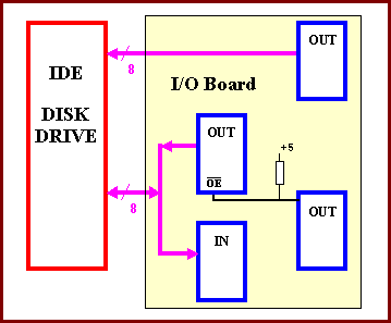
The access to the IDE hard disk would be simple if the Core Board had a second, not used, PIA. A separate circuit
board that piggy-backed the PIA on the Core Board and added one extra PIA would be a possible solution, but with
software overhead it is possible to connect the IDE disk to the I/O Board.
The lower 8 databus bits [D0:7] are connected to an output port *AND* an input port in
parallel. Since the output ports on the I/O Board are always enabled, a patch is required so that the output port
can be set into 3-state mode so that reading data from the IDE disk is possible without shorting the databus against the
output port.
The patch requires one bit from an extra output port; the OE* pin of the output latch used for the
bi-directional databus is cut from its GND connection and it is wired to that single bit of the extra output port.
The 8 input-only signals (RST*, RD*, WR*, CS1*, CS0*, A2, A1, and A0) are directly tied to an
output port of the I/O Board.
The IRQ, ACT*, the upper 8 databus bits [D15:8] and a few other pins of the IDE
disk drive are not connected to the I/O Board. Not using the upper 8 databus bits means that half of the disk capacity
will not be used, but who wants more than a few Mb's on a pdp8/e anyway ... it saves one output port and one input port.
If you insist on using the full capacity of the disk (for an other project) you must make some minor changes in the
driver software and add the two extra ports in hardware.
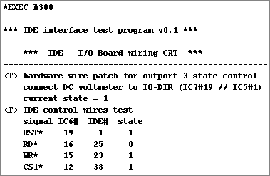 The draft version of the low-level routines to read and write to the disk's registers did not work ... the big question:
is the software not correct or did I make an error in the hardware? To find out I wrote some extra code to test each
output pin. When the program runs it accepts just 4 keyboard entries:
The draft version of the low-level routines to read and write to the disk's registers did not work ... the big question:
is the software not correct or did I make an error in the hardware? To find out I wrote some extra code to test each
output pin. When the program runs it accepts just 4 keyboard entries:
- "1" -> make the output pin +5 V.
- "0" -> make the output pin 0 V.
- CR -> move on to the next pin
- ESC -> stop the program
When using this testcode, it is safer to disconnect the IDE hard disk from the connector ...!
As one output is checked at a time, a simple DC voltmeter is all you need to test the output pins.
I connected the voltmeter to the pins on the IDE connector; that way I also checked the cable!
To test the input pins connect a momentary switch to the pin under test. The switch connect the pin either to
GND or to +5 Volt.
The testcode displays continuously the logic level it reads from the pin under test, and accepts only the
CR or the ESC key.
Warning
The approach of using the available I/O Board for interfacing the IDE disk needs some special attention for the
software implementation. I try explain this here. The I/O Board is a resource of the system, and as such, needs
controlled access. It must be prevented *at all time* that for example the console (FIRQ routine!) and some disk access
routine are using the I/O channel(s) at the same time as they can change the data transport direction of the I/O control.
In fact, all *access sequences* to the I/O Board are mutually exclusive and must be completed before any other process
may use the I/O Board.
Some ideas for the future
One input port of the I/O Board is not yet used. That port could be used to read the position two switches, LOAD/RUN
and WRITE-PROT, as found on the RK05 disk drive ... The not used bits of the output port that controls the
bi-directional databus to the disk drive could be used to drive a few LED's as found on the front panel of the RK05.
The "WRITE" and "READ" light can be made with TTL logic from the WR* and RD*
signal, gated with the ACT* signal (pin #39) of the IDE disk drive.
Expected performance of the IDE disk drive
Any requested disk access will need to change the I/O data transfer direction several times. For example: to *write*
a command to the disk, the software must first check the disk's status by a *read* operation. After the command is
written, again it is necessary to check the status (data request/available), etc. To keep things simple all routines
set the I/O data transfer direction explicit, but a flag indicates if the I/O data transfer direction change is required.
Anyway, the IDE disk will be a lot faster than the BIN loader ...
December 1st, 2004 was a day to remember in more than one way ...
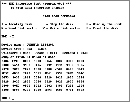
I finished implementing the "upgrade" from an 8 bit to a 16 bit data path because it was nagging me that the response
of the "IDENTIFY" command could not be interpreted as I missed half of the data.
I could write 256 bytes to a disk sector and, when read back, I got the same data, so that was promising.
Then I read how the pdp8 writes data to the RK8-P Disk Interface. Every sector of the RK drive provides storage
capacity for
- 2 12-bit header words
- 256 12-bit data words
- 1 12-bit parity word
With the 8-bit data approach I would need 3 'real sectors' to implement one "pdp8 sector".
To implement the RK8-P Disk sector only 2 real sectors are needed with a 16-bit data path.
The software to access the IDE disk are almost finished. I still have some sort of timing or handshake problem.
After executing the IDENTIFY command I can not issue a new command. The software "hangs". Most
likely, the software is polling the BUSY or the READY bit which keeps the
wrong status.
If you are interested, here is the IDE disk version 0.2 software
idedisk-02.zip (version 02dec2004, 21 kbytes).
All the information you need to get started is in this file. I'll appreciate any feedback!
As you can see, there are a lot of wires from the I/O Board. Using colored wires makes building it all easier and
less fault sensitive.
Putting it all together (IDE disk and pdp8/e simulator)
The main requirement to make the IDE disk accessible to the pdp8/e simulator is that the implementation must be
transparent, that is, when the pdp8/e software issues an IOT, some mechanism must perform the actions.
Since there is a blinkenlight console the disk access must be visible, and that is possible! When the Indicator
Selector Switch (the knob) is set to "STATE" the LED BRK or
BRK PROG must be turned on, as on a real pdp8/e console. (I do not yet know which one
is the correct one).
There are 3 pieces of software that play a role in the mechanism: the pdp8/e simulator, the IDE disk routines
and the Fast Interrupt routine (FIRQ). The FIRQ handles all console activity, the switches and the LEDs. Thus,
the FIRQ routine accesses the I/O Board and changes the I/O direction between the I/O Board and the PIA
on the Core Board. This means that during any disk access the FIRQ must be disabled! So a "trick" is needed to
get the BRK or BRK PROG LED turned on. The solution is a flag [accide] to
create a form of communication/handshake between the FIRQ routine and the IDE access routines. In pseudo code
it looks like this:
   pdp8/e simulator                   IDE access code                  FIRQ routine
------------------------------------------------------------------------------------------------
[accide] := $00 (initialisation)                                  (enabled: runs every 20 msec)
IOT read/write disk executed
1. build parameter packet                                           if [accide] == $80
2. call the IDE function            1. [accide] := $80                 set [brkact]
  (pdp8/e sim looses the CPU)       2. wait until [accide] == $01      [accide] := $01
                                    3. disable FIRQ
                                    4. perform IDE disk action      if [accide] == $00
                                    5. store status in packet          clear [brkact]
                                    6. [accide] := $00
                                    7. enable FIRQ                  if [brkact] == set
                                    8. return to caller                turn on BRK LED
3. continue from IOT                                                else turn off BRK LED
   process returned status
|
The [accide] flag (access IDE) is initialised to $00 at startup. When the pdp8/e simulator code executes
an IOT for the disk device, the simulation software builds the appropriate parameter packet and calls the
required IDE device access function.
The IDE device access functions all have two tasks, the first is of course the actual disk I/O but it
must also make sure that the BRK or BRK PROG LED is turned on.
Since the FIRQ flag is set (disable) by the disk I/O routines to make sure that there is exclusive access
to the I/O Board, the [accide] flag acts as a communication/handshake mechanism. The IDE device access
functions set the msb of [accide], and then waits until the msb of [accide] is cleared, and the lsb is
set. When this action occurred it means that the FIRQ routine has seen the msb of [accide], which is the
signal to turn on the LED. Thus, the FIRQ routine has done its task and the IDE device access functions
can disable the FIRQ and execute the disk I/O function. To signal the completion (and complete the cycle
back to its start condition) the IDE device access functions reset the [accide] flag and enable the FIRQ
again before returning to the caller (the pdp8/e simulated IOT instruction). As the FIRQ routine is
executed at the next timer interrupt (20 msec interval), it detects that [accide] is zero and will turn
off the LED.
Since the LED is part of one of the (simulated) pdp8/e registers, the [accide] flag does not turn on
the LED directly, but the LED action is done through an extra flag, [brkact]. The part of the FIRQ code
that determines which LEDs must be turned on evaluates the [brkact] flag only if the Indicator Selector
Switch (the knob) is set to "STATE".
Here you see my first attempt to run the Disk Monitor System (DMS) Builder software,
DEC-P8-SBAF-PB.BIN.
The messages are identical to the ones in the manual, so things start promising, but I will have some
debugging to do ... somewhere!
The line at the bottom that starts with [t] is a trace debug output
line that I added to notify how far I get.
 To debug the system I can put a breakpoint in the 6809 code, but I would like to have a mechanism
to step through the pdp8 code too. Since the SING STEP switch on the console was not
used, but had the same function as HALT switch, I changed that.
The CONT momentary switch now works as follows:
To debug the system I can put a breakpoint in the 6809 code, but I would like to have a mechanism
to step through the pdp8 code too. Since the SING STEP switch on the console was not
used, but had the same function as HALT switch, I changed that.
The CONT momentary switch now works as follows:
- HALT active --> step through pdp8 program, instruction-wise.
- SING STEP active --> as HALT, but after each step the
registers are printed.
The function on a real pdp8 would step through the cycles of an instruction, but that is not
really useful in the simulation. When all operates the way it should, I will add the cycle step
details in conditional assembly. If that functionality is wanted it can be activated by assembling
the code with one changed flag.
The cycle step simulation is default not activated because
of the performance penalty for the entire simulator.
The DF32 seems to work, the mentioned Builder program writes information to the disk. The Builder
finishes correctly because it prints the dot (.) prompt which indicates that the Disk Monitor is ready
to accept commands. I have not yet had the time to do more checks and copy other programs from paper
tape through the DMS Loader onto the "DF32". Each time a data transfer is done (execution of the
DMAR or DMAW IOT), the BRK and
BRK PROG turns on and off. I have choosen to turn on / off both LEDs.
The stuff looks promising ...!

Up till now I used the "BIN loader" that is implemented in the simulator (6809) code which operates
at 9600 Bd. With the DMS, the Loader is pdp8 code (simulated), thus it can not run at that speed.
Without a hardware modification it is possible to drop the speed to 2400 Bd. That is not a common
baudrate for terminals, so if that poses a problem a small capacitor must be added to the Core Board
to drop the speed to 1200 Bd. The Core Board provides the connection for an extra parallel capacitor!
Making a replica of the PDP-8/e console - step 3
While I work on the software, it does not mean that the actual construction is stopped!
Measurements were taken and draft views were drawn. The electronics, Core Board, I/O Board,
console with switches and LEDs and a small PC power supply are not heavy enough. The complete
pdp8/e simulator should stay put when you push the switches. So I started with the bottom of the
box: 362 x 300 millimeters aluminium ... 10 mm thick. That gives some weight :~)
Two stand-offs are at the front side to install the frontpanel, not the plate with the
switches and the LEDs.
The frontpanel is made of the following layers:
1. transparent perspex, thickness 1 millimeter
2. 600 dpi (toner) color print on white paper
3. transparent perspex, thickness 1 millimeter
4. a frame of 12 x 12 millimeter aluminium rod
Both the perspex plates have holes for the switches. The four parts are held together with bolts
that are mounted from the rear side. The frame is made of four rods that are mounted together
with 4 screws, one at each corner.
I am not going to waste a lot of bandwidth to show all the steps. I leave that up to your
inventiveness, but here is my result, and believe me this is not a job done in one evening!

Hardware issues and debugging!
At this stage I discovered that the base plate surface (36x30 cm) is too big to my liking. The
front width is 36.2 cm and I am not going to change that! The depth, however, could easily be
made half of what it is now, and because of the weight of the base plate you can still push
the switches and the unit stays rock-solid at its place. To decrease the depth I ordered a
CompactFlash to IDE interface on eBay. They are cheap at $1, but the shipping cost are $10 ...
I have an old 16 Mb CF card that would fit nicely in the pdp8/e simulator. When the CF card
operates (to be determined) I can get rid of the mechanical vulnerable IDE hard disk, and
the +12V, thus the PC power supply can be swapped by a small +5V only power supply
... we'll see!
Back to the simulation software.
As told, the Builder finishes and puts out the 'dot' prompt. When I enter an invalid command
there is no response anymore, and the ADDRESS LEDs blink is a typical pattern.
After a hard reset of the 6809 I always find the same (pdp8) PC value, or a PC that is in a very
close range. I must find out what is expected, because it is clear that the pdp8 software is
running a small loop, testing a flag ...
Reading the ADDRESS LEDs on the front panel I found out that the Program
Counter (PC) loops in the range o7200-o7206 octal. After resetting the 6809
processor, I find in the memory location 'PC' the value $0E82 (hex). That checks out as o7202 =
$0E82.
The core memory fields of the pdp8/e simulation start from address $2300 in the
6809 RAM space. Also, remember that a 12-bit word in core corresponds with 2 bytes in RAM.
To find the real address in RAM you must multiply the core address by 2 and add $2300.
The address $0E82 (o7202) corresponds with $4004 in RAM (do the math).
After one evening debug activities I was fed up with all that conversion work. Octal to hex, hex
to octal, multiply by 2 and adding $2300 took too much time before I could start reasoning about
the things I saw. So, I wrote a quick hack: a small 6809 program that does a crude disassembly
of the pdp8 instructions. I added the PDP8 hex and octal values in the output and the real RAM
address to make life easier.
I plan to add the pdp8 disassembler program in the
EPROM when I burn the simulator code too.
The command entry requires an address specification
in CORESYS syntax (addr1:addr2 or addr1!count or addr1).
Note that the specified address must be a pdp8 core address!
This is the disassembly output after the following steps:
- load pdp8/e simulator code
- EXEC A300 (start simulator)
- for the loader: load DEC-D8-SBAF-PB (the Builder 'papertape')
- after loading, enter ^Q and say "N" to the "more .BIN to load?"
The simulator now waits for depressing the "CONT" switch.
- I press the 6809 RESET button.
- Load the pdp8dis program and start it to see the code before the simulator executed it:
*EXEC BC00 0E80!10

  $4000  ($0E80 / o7200):   $06E6 / o3346  DCA    $0EE6 / o7346   ($40CC)
  $4002  ($0E81 / o7201):   $03E3 / o1743  TAD i  $0EE3 / o7343   ($40C6)
  $4004  ($0E82 / o7202):   $04E3 / o2343  ISZ    $0EE3 / o7343   ($40C6)
  $4006  ($0E83 / o7203):   $0F28 / o7450  SNA
  $4008  ($0E84 / o7204):   $0A80 / o5200  JMP    $0E80 / o7200   ($4000)
  $400A  ($0E85 / o7205):   $0681 / o3201  DCA    $0E81 / o7201   ($4002)
  $400C  ($0E86 / o7206):   $03E3 / o1743  TAD i  $0EE3 / o7343   ($40C6)
  $400E  ($0E87 / o7207):   $0682 / o3202  DCA    $0E82 / o7202   ($4004)
  $4010  ($0E88 / o7210):   $02E8 / o1350  TAD    $0EE8 / o7350   ($40D0)
  $4012  ($0E89 / o7211):   $08EE / o4356  JMS    $0EEE / o7356   ($40DC)
  $4014  ($0E8A / o7212):   $0ED6 / o7326  CLA CLL CML RTL
  $4016  ($0E8B / o7213):   $02F3 / o1363  TAD    $0EF3 / o7363   ($40E6)
  $4018  ($0E8C / o7214):   $06E3 / o3343  DCA    $0EE3 / o7343   ($40C6)
  $401A  ($0E8D / o7215):   $02E7 / o1347  TAD    $0EE7 / o7347   ($40CE)
  $401C  ($0E8E / o7216):   $0683 / o3203  DCA    $0E83 / o7203   ($4006)
  $401E  ($0E8F / o7217):   $0281 / o1201  TAD    $0E81 / o7201   ($4002)
*
|
Now, the steps are repeated, but the Builder program is executed and a command is entered
at the 'dot' prompt.
These are the steps:
- load pdp8/e simulator code
- EXEC A300 (start simulator)
- for the loader: load DEC-D8-SBAF-PB (the Builder 'papertape')
- after loading, enter ^Q and say "N" to the "more .BIN to load?"
The simulator now waits for depressing the "CONT" switch.
- I press the "CONT" switch and answer the questions the Builder asks.
After several disk write and two disk read accesses the 'dot' prompt is printed.
- I enter a command, followed by CR.
The code executes four disk read accesses and then the loop is entered.
- I press the 6809 RESET button.
- Load the pdp8dis program and check the code:
*EXEC BC00 0E80!10

  $4000  ($0E80 / o7200):   $06E6 / o3346  DCA    $0EE6 / o7346   ($40CC)
  $4002  ($0E81 / o7201):   $0101 / o0401  AND i  $0001 / o0001   ($2302)
  $4004  ($0E82 / o7202):   $034C / o1514  TAD i  $004C / o0114   ($2398)
  $4006  ($0E83 / o7203):   $0000 / o0000  AND    $0000 / o0000   ($2300)
  $4008  ($0E84 / o7204):   $0A80 / o5200  JMP    $0E80 / o7200   ($4000)
  $400A  ($0E85 / o7205):   $0681 / o3201  DCA    $0E81 / o7201   ($4002)
  $400C  ($0E86 / o7206):   $03E3 / o1743  TAD i  $0EE3 / o7343   ($40C6)
  $400E  ($0E87 / o7207):   $0682 / o3202  DCA    $0E82 / o7202   ($4004)
  $4010  ($0E88 / o7210):   $02E8 / o1350  TAD    $0EE8 / o7350   ($40D0)
  $4012  ($0E89 / o7211):   $08EE / o4356  JMS    $0EEE / o7356   ($40DC)
  $4014  ($0E8A / o7212):   $0ED6 / o7326  CLA CLL CML RTL
  $4016  ($0E8B / o7213):   $02F3 / o1363  TAD    $0EF3 / o7363   ($40E6)
  $4018  ($0E8C / o7214):   $06E3 / o3343  DCA    $0EE3 / o7343   ($40C6)
  $401A  ($0E8D / o7215):   $02E7 / o1347  TAD    $0EE7 / o7347   ($40CE)
  $401C  ($0E8E / o7216):   $0683 / o3203  DCA    $0E83 / o7203   ($4006)
  $401E  ($0E8F / o7217):   $0281 / o1201  TAD    $0E81 / o7201   ($4002)
*
|
... the addresses o7201, o7202, and 07203 are changed !
All through this project I have had lots of support from Vince. He has way more knowledge
about the PDP8 than I will ever have. Before I go ahead it is time to fix a few small bugs
that are annoying during the debug process. When I push "CONT" it also
loads the setting of the SWITCH REGISTER into the PC.
That makes running the MAINDEC pdp8/e instruction tests diagnostics
impossible. Further, I modified the disassembler so that OPR group 1 and group 2 are decoded to
the instructions such as CLA and SZA, but it prints the
wrong mnemonics. That's not much of a help ...!
(The link downloads the corrected version.)
Intermezzo
I received the CF CompactFlash to IDE hard drive adapter.
It shipped from Hong Kong to The
Netherlands in just 5 days!
I removed the IDE hard disk drive and connected the adapter card, inserted a CompactFlash card
of 32 Mb, and ran the small IDE test program.
Here is the result of the IDENTIFY command output.
As you can see, the C/H/S values are different, so you must change the parameters that reflect
this disk's properties :
[SPC] (Sectors per Cylinder) and
[SPT] (Sectors per Track).
Since we have no listing of the Builder program, we used the MAINDEC-08-D5DB-D
DF32 Multi Disk diagnostic program.
Although it is not really a diagnostic program it proved very useful.
Remark: the "IOT DMAR ...." is debug output to follow the program execution.
We (Vince and I) found the following problems with the DF32 simulation code:
- Interrupt request flag
At the completion of an I/O transfer it is not enough to set the TRC
interrupt flag (TRansfer Complete) for the simulator.
In the variable IOflgs you must set an interrupt request flag that has been
allocated for the source (DF32 device).
After that was implemented, we got the following output:
4 EXISTENT DISK(S)
IOT:DMAR  df23WC = $0C00  df32CA = $033F  ... df_irq = $00  df_sts = $00
UNDEF. INT.
UNDEF. INT.
UNDEF. INT. |
The message "UNDEF. INT." is repeated until I press the 6809 RESET button.
Vince suggested that the interrupt request stays active. The interrupt flag TRC in
the status word is cleared but the interrupt request flag itself is not, thus the interrupt immediately
recurs, but the disk no longer indicates an operation completed.
That remark hit bulls-eye!
At the start of the DMAR, DMAW, and the
DCMA IOT must clear the interrupt request flag, which they did not ...
That explains the undefined interrupt messages that keep coming. Now the output is:
4 EXISTENT DISK(S)
IOT:DMAR  df23WC = $0C00  df32CA = $033F  ... df_irq = $00  df_sts = $00
IOT:DMAW  df23WC = $0C00  df32CA = $073F  ... df_irq = $00  df_sts = $00
IOT:DMAR  df23WC = $0C00  df32CA = $0B3F  ... df_irq = $00  df_sts = $00
TA0000 WC 0000 GD 1042 BD 7402
TA0000 WC 0001 GD 2104 BD 7402
TA0000 WC 0002 GD 4210 BD 7402
TA0000 WC 0003 GD 0423 BD 7402
TA0000 WC 0004 GD 1046 BD 7402
|
The output goes on and on. A short explanation is perhaps in place of the DF32 Multi Disk
diagnostic.
It reads a sector, then writes data patterns to that sector. After the write operation the sector
is read again and the data is compared. If all is OK, the original data of the sector is written
back to the disk, and the next sector is tested.
NOTE: "TA" is Track Address, "WC" is Word Count (word in sector), "GD" is
data written, and "BD" is data read.
Typical is that the data read is always o7402.
That is the octal code for the HLT instruction,
and at start up of the simulator all Fields are initialised with that value!
- Code bug
The translation between pdp8/e core memory (12-bit words) and 6809 memory (8-bit bytes)
the core address must be multiplied by 2 to get the correct 16-bit word in 6809 address space.
However, the code multiplied by 2 also the base address value of the pdp8/e Field. The fix is
easy, and this is the result:
4 EXISTENT DISK(S)
IOT:DMAR  df23WC = $0C00  df32CA = $033F  ... df_irq = $00  df_sts = $00
IOT:DMAW  df23WC = $0C00  df32CA = $073F  ... df_irq = $00  df_sts = $00
IOT:DMAR  df23WC = $0C00  df32CA = $0B3F  ... df_irq = $00  df_sts = $00
IOT:DMAW  df23WC = $0C00  df32CA = $033F  ... df_irq = $00  df_sts = $00
IOT:DMAR  df23WC = $0C00  df32CA = $033F  ... df_irq = $00  df_sts = $00
IOT:DMAW  df23WC = $0C00  df32CA = $073F  ... df_irq = $00  df_sts = $00
|
Again, the output goes on and on ... reading / writing / reading / checking / writing sectors.
The DF32 Multi Disk manual says that you can stop the process with ^C (Control-C), so I did.
IOT:DMAR  df23WC = $0C00  df32CA = $033F  ... df_irq = $00  df_sts = $00
IOT:DMAW  df23WC = $0C00  df32CA = $073F  ... df_irq = $00  df_sts = $00
IOT:DMAR  df23WC = $0C00  df32CA = $0B3F  ... df_irq = $00  df_sts = $00
IOT:DMAW  df23WC = $0C00  df32CA = $033F  ... df_irq = $00  df_sts = $00

Program halt (HLT microcode in OPR instruction)
 Df=0 AC=0000 L=1 MQ=0000 U=0 ION=0 NoI=0 Ireq=00000
 If=0 PC=0151 In=7402
|
Just as described in the manual the diagnostic completes the current read operation, and
writes the original data back to disk before the DF32 test program stops at the programmed HLT!
It looks like the simulation of a DF32 system and three DS32 disks on
the IDE hard disk operates correctly!
Installation of DMS - Disk Monitor System
After loading the pdp8/e simulator, I did *not* load a .BIN file, terminated the download
immediately with ^Q (control-Q) and answered "N".
I used the console switches to load the bootstrap for the DF32
Random Access DECdisk File.
The bootstrap code is listed at the right.
Then I used the console switches to set the start address at octal 0200, lifted the
HALT switch and pressed CONT.
I got the <0> and the dot prompt!
|
    memory    data    symbolic
  ---------------------------------
                       *0200
     0200     6603     DMAR
     0201     6622     DFSC
     0202     5201     JMP    .-1
     0203     5604     JMP I  .+1
     0204     7600     7600
                       *7750
     7750     7576     7576
     7751     7576     7576
|
|
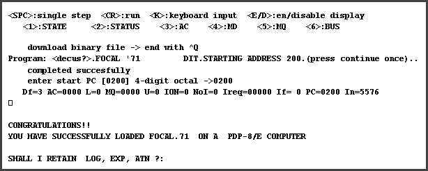
*EXEC A300

*** pdp8/e  SIMULATOR  v0.5 - 05jan2005 ***

[i] initialising pdp8/e core memory fields ... ok
[i] initialising Real Console hardware     ... ok
[i] initialising IDE hard disk interface   ... ok
    download binary file -> end with ^Q ... completed succesfully
    load another .BIN  [Y/N] : N
<0>
.LOAD

*IN-T:

*
ST=
^
|
Then I entered the "LOAD" command to bring in the binary loader.
The loader prompts for the input device by the *IN- where I enter T:
for the slow-speed papertape reader.
The device is accepted which is indicated by the * on the next line. The start
address is prompted by the ST= , which does not need any data in this case. On the next
line, the first up-arrow indicates that the loader is ready to load the "paper tape".
Then I sent the DEC-D8-PDAD binary, and I see the LEDs flash on the console,
but I do not get the second up-arrow that would indicate that the load completed ...
I am quite sure that the 9600 Bd baudrate is too fast for the binary loader which is
executed by simulating pdp8 instructions on the 6809! The ACIA can of course accept a byte at 9600 bd,
but the .BIN loader that accepts and processes the received data is the pdp/8 simulated code. If only
I could insert a delay between every byte to be sent, to allow enough processing time ...
I got fed up with the cumbersome Hyperterm / disconnect and then load the .BIN file via a
'DOS-box' with TYPE filename > COM1: and then connect again in
Hyperterm. I found a program called Terminal which I am using now. It works perfect!
Check it out at
Bray's Terminal Home Page .
I loaded the FOCAL71 program via Terminal and where Hyperterm fails miserably, Terminal passes perfect!
The author is very responsive, and he is already working on a configurable "delay between bytes sent" option!
Making a replica of the PDP-8/e console - final step
Time again to change focus from the software to the hardware, to get fresh ideas.
I still had to make the rear side, and a short inventory showed the components that I needed:
- power supply +5V for the electonics and +12V for the hard disk
- DE-9 connector for console (COM: port to the PC)
- reset button and a small button to select the power-up mode
- mains power switch, fuse, and and power connection
- 37-pin D "feature" connector for future expansion ...
Up till now I used an old power supply from an 286 PC-AT computer, but that's a bit bulky. I saw the new
small PC's, so there must be smaller power supplies available too. Search for "Flex ATX" and you will
find several sources.
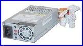
These power supplies are small [4 x 8 x 15 cm] and (that is ATX standard) they have a connection
that allows a low-voltage switch to turn on the PSU. In fact, the power supply is sort of "ON"
as soon as AC is applied, but that is only +5V stand-by (rated at 1.5A already).
The green wire of the ATX connector is called "PS-ON", it is pin #14.
(warning: the pin numbering of the ATX connector is not what you would expect)!
Again, search for "ATX Power Connector" to find the details.
Anyway, if you connect the green wire to GND
(any black wire), the power supply turns on.
So, I wired a black and the green wire
to the front panel switch. I was not able to find a small key switch that could switch 230VAC, but this
low-voltage key switch with the PS-ON wire does the job nicely, just as in regular PC's nowadays.
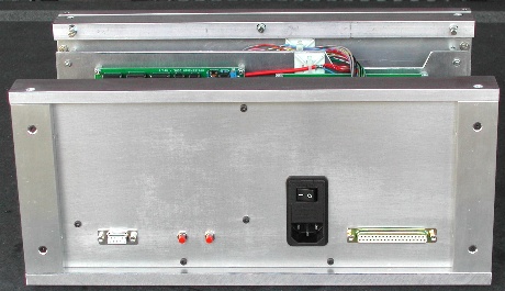
The rear side of the pdp-8/e simulator
The 37-pin D connector is installed "just in case" I have future expansion ideas. I will only need to
solder the wiring to the connector without any disassembly and drill work. Actually, some 'wild' idea
is the connection of replicated RK05 disk drive front panels with the lamps and the 2 switches, which
are of course under control of the pdp8/e simulator ...
Here are a few other pictures that show the inside of the simulator, the Compact Flash card and the
construction of the front panel "sandwich". Click on them for a larger view!
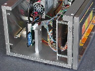
left side, Compact Flash card
800 x 595 [224 kb]
|
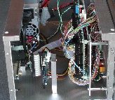
left side, some wiring
800 x 679 [263 kb]
|
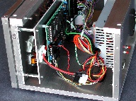
right side, ATX power supply
800 x 595 [250 kb]
|
Giving the PDP-8/e useful disk space
I read that the DF32 was mostly used as a 'fast' swap file. If you want to do more useful actions
on a pdp-8/e, you needed a bigger disk. The DF32 controller with one DS32 disk offers 32Kw space,
and the maximum configuration with four DS32 disks attached gives you 128 Kw.
To run OS/8 you need a bit more space, and Vince mentioned the RF08 controller.
The RF08 is very similar to the DF32, in fact the DF32 and the RF08 share some of the IOT
instruction codes, although not all of these IOT's do exactly the same operation. Also, the RF08
has a few more IOT's. The RF08 with one RS08 gives 256 Kw disk storage, and here the maximum
configuration is also four RS08 disks, thus a whopping 1024 Kw disk space!
In just 7-8 evenings I added the RF08. I implemented that code with a conditional assembly flag
called RF08dev. When that flag is set to zero the assembly output supports
the DF32 controller with four DS32 disks, if the flag is set to one, the code offers the RF08
controller with four RS08 disks.
 .PIP
 *OPT-L
 *IN-S0:

 FB=1527
 NAME  TYPE    BLK
 AF
 PIP .SYS (0) 0025
 EDIT.SYS (0) 0016
 LOAD.SYS (0) 0011
 .CD..SYS (0) 0007
 .OS..SYS (0) 0025
 FORT.SYS (0) 0010
 FOSL.SYS (0) 0007
 STBL.SYS (0) 0001
 DIAG.SYS (0) 0004
 .FT..SYS (0) 0035
 .DDT.SYS (0) 0022
 DDT .SYS (0) 0002
 *OPT-L
 *IN-S1:

 FB=1756
 NAME  TYPE    BLK
 AF
 *OPT-
| |
In the PIP listing output you can see the first system programs loaded onto the disk S0:.
The second RS08 disk (S1:) is still empty.
I still have not solved the BIN loader problem, but you can load these programs also with the 6809 BIN loader
in the pdp8/e simulator. After you loaded the simulator itself (S19 file) and started the simulator, the
simulator prompts for a .BIN file. Then you send one of the programs from the terminal to the simulator.
When the file is sent, enter control-Q and answer "N" to the question to load another file.
The trick now is to keep the file in "core". Push the HALT switch down, set the
SR to the value 0o0200, and then push (momentary) down the ADDR LOAD
switch.
These actions load the bootstrap code into "core" and set the PC to the correct value.
Lift the HALT switch up and simply push (momentary) down the CONT switch.
DMS is started. At the dot prompt enter the SAVE command for the loaded program.
That is all -- one caveat: the program that you want to save to disk must not use the same 5 locations where the
bootstrap is loaded because they get overwritten!
The 5-word bootstrap code is loaded at the address indicated by the
SR when you push the ADDR LOAD with the described switch sequence. Also,
make sure that these words are not overwritten by the data read from disk! And, the 5 words must all be
in the same page as the SR value is used to relocate the two JMP instruction
target addresses.
The latest modification is the access method of the disk. As I am using a Compact Flash card, I really do not need
the old-style C/H/S access of the IDE disks, but can use the LBA access of modern disk drives. The translation from
a sector number (in the pdp8/e code) to the physical disk location (CHS or LBA) is done in one routine, called
SetLBA. That routine is now transparent: the sector number = LBA.
Click here to get that latest version .
|
The simulator now supports a few command line switches.
- -v "verbose"
The simulator environment operates silently.
If the "-v" switch is specified, the simulator will generate a few messages on the start-up.
- -c "core"
Default, all allocated memory space is erased and filled with HLT instructions, thus the
memory acts as if it is MOS memory. If you specify the "-c" switch, the memory behaves as if it is real core
memory and the allocated memory space is not erased. This behaviour can be useful if you want to (6809) reset the
system and start the pdp8/e simulator again keeping the loaded program in core intact.
- -t "tracing"
The tracing facility is activated.
For more details, see the Boot and run OS/8 chapter near the end of this page. The "-t" switch was added later in the project.
- -d# "disk"
Since the hard disk or the Compact Flash card can easily be a lot bigger than the maximum pdp8/e configured disk space
(RF08 with 4 RS08 disks which is 1024 Kw), you can have several configurations on one physical device. Only one
"disk" can be visible. The "#" is a number between '0' and '9' (both inclusive), where '0' is the default value.
You can have, for example, on disk #0 (-d0) DMS installed with a Fortran environment, on disk #1 (-d1) DMS installed
with a PAL environment, on disk #2 (-d2) OS/8 installed, etc.
- -byyy "boot"
While mentioning Operating Systems and having plenty of disk space with the "-d" option, the "-b" command line
switch allows you to specify which Operating System bootstrap must be enabled. Of course, the OS bootstrap that
you select must be installed on the disk that you specified. At this moment "yyy" can be "DMS" or "OS8".
Note: both the Operating System bootstrap identifiers must be entered in uppercase.
The command line switches may be entered in lowercase or in uppercase. The order is not important, however,
the command line switches must be separated by exactly one space. The "-v", "-c" or "-t" option can be specified more
than once, the result is always that the option is turned on (no toggle function). If the "-d" or "-b" option
is specified more than once, the last entered option is active.
Installation of OS/8
The final step of this pdp8/e homebrew project is the installation of OS/8 in the simulator.
The approach here is to use a PC, and run the SIMH pdp8 simulation on the PC. In the
SIMH environment you create and fill the virtual RF08 disks with OS/8 (and the nice programs that
you want to use, like BASIC, Adventure, and of course some variant of the ever popular StarTrek implementations).
After that is done, you simply transfer the virtual disk to the pdp8/e simulator.
Here is how I did it, again with some help from Vince when I got stuck.
- 1. Get the necessary files
- I found the following, very useful, site
http://www.pdp8.net/images/images/misc_dectapes.shtml .
You need these two files to get going :
- AL-4711C-BA.tu56
- AL-4712C-BA.tu56
but there are more very interesting files!
For documentation go to
http://www.classiccmp.org/bitsavers/pdf/dec/pdp8/ and get
- OS/8 System Generation Notes (AA-H606A-TA_os8SysgenNotes.pdf)
- CHAPTER 9 BUILD (OS8_Handbook_Apr1974.pdf)
Again, there is more useful information to read.
Search the well-known sites for more documentation (and files)!
- 2. Create the RF08 disk with OS/8
- For simplicity, I copied all the needed files to the same BIN directory where the
PDP8.EXE is.
The following description is based on using a PC. --
Open a "DOS" box, and goto the BIN directory of SIMH.
First, make a copy of the original DECtape images because SIMH reads them and when you terminate
SIMH the images are written back to disk! You want to preserve the orginal files. Also, use the
disk generation utility gendisk to create a RF08 disk container file.
gendisk needs the "-f" command line switch which specifies the output file name. Default, gendisk
creates a file of exactly 1k (1024) bytes, all zeroes. With the second command line switch "-s" you can specify
the file size to be an integer number of times 1k. The RF08 with four RS08 disks can hold 1 Mword, thus 2 Mbytes.
So, at the DOS prompt, enter the following commands :
   C:\BIN>copy  AL-4711C-BA.TU56  OS8.TU
   C:\BIN>copy  AL-4712C-BA.TU56  OS8DVC.TU
   C:\BIN>gendisk -frf4dsk.rf -s2048
|
Enter 'pdp8' at the DOS prompt to start the SIMH pdp8 simulation.
At the SIMH prompt enter the following commands :
(the responses from SIMH are not shown)
   C:\BIN>pdp8
   simh>set df disable
   simh>set rf enable 4P
   simh>att dt0 os8.tu
   simh>att dt1 os8dvc.tu
   simh>att rf rf4dsk.rf
   simh>boot dt0
|
In a short moment you will get the "." dot prompt of OS/8. That's all to get OS/8 running in SIMH.
Note that the RF4DSK.RF file does not exist! It is created in memory and will be saved to disk when
you terminate SIMH.
Next action is adding the RF disk to the SIMH configuration. Enter the following OS/8 commands :
   .RUN SYS BUILD
   $LOAD DTA1:RF08NS.BN
   $INSERT RF,RF=4
   $BO
   .SAVE SYS BUILD
   .ZERO RF:
|
The new RF08 is a so-called non-system disk, the RF08 can not be the SYS volume.
We must make the RF08 disk a system disk, and these actions will do just that :
   .RUN SYS BUILD
   $UNLOAD TC08
   $LOAD DTA1:RF08SY.BN
   $INSERT RF08,SYS=4
   $BO
   WRITE ZERO DIRECT?YES
   .SAVE RF NBUILD
|
Now, immediately reboot from DECtape to copy all the desired files to the RF08 disk. When you have all the
files on the RF08 (including NBUILD), boot the RF08, and copy NBUILD.SV to BUILD.SV. Here are the commands :
   .^E
   simh>boot dt0
   .COPY RF:*.*<*.*
   .COPY RF:BUILD.SV<RF:NBUILD.SV
   .DELETE RF:NBUILD.SV
   .^E
   simh>quit
|
The ^E (control-E) stops the pdp8 simulation and takes you back to the SIMH prompt. As you saved
the configuration to NBUILD.SV, the old BUILD.SV still exists. So, you can
boot again from dt0: and then copy the files. Returning to SIMH is essential! After the
SAVE RF:NBUILD, the OS/8 BOOT command is not valid anymore this condition!
Remark. After SIMH is booted into OS/8 and you stop SIMH again,
SIMH writes the file out.
You must specify the "set rf enable 4P". Otherwise SIMH sets the size back to
256K, which will cause I/O errors when OS/8 accesses data past the 1023rd block.
- 3. Translate the RF08 disk to "transportable" files
- Now you have a maximum configured (4 RS08 disks) RF device on your PC which must be moved into the simulator.
As the simulator does not have a file system (desides the Operating Systems ones in the pdp8 simulation) you need
some sort of utility to transfer the whole (disk)file. "dumprest" can do this.
Basically, dumprest consists of two programs, one runs on the host (PC), and the other runs on the client
(pdp8).
However, in this case it is not a real pdp8 but the simulation pdp8, and one thing is sure: it
will fail at a data transfer rate of 9600 Bd. Since 2 Mb (1 Mword for a maximum configured RF08) takes too
long at 300 Bd, I made a utility that can transfer the bytes at 9600 Bd, the maximum speed for a 6850 ACIA.
The PC utility bin2s19 accepts one input file and produces a number of
output files in Motorola S19 record format.
The 6809 CORESYS monitor understands the S19 records, so the generated output files can be sent to the 6809 system.
As the output is at least twice the size of the input file, the output must be split into chunks that the 6809
system can handle. That size is limited by the amount of RAM free to store the S19 to binary converted data in, so
bin2s19 generates output files of (converted into binary) 32k bytes. The S19 record (ASCII) file size will be 77k.
The names of the output files are indentical to the input file name with two attached extensions. The first extension
is a sequence "number", the seconds extension is "S19". The sequence number is a letter (A-Z) with a number (0-9).
   C:\BIN>bin2s19 -frf4dsk.rf -i -s1000
     -> input file  rf4dsk.rf  Intel->Motorola
     -> output file rf4dsk.rf.A0.S19   SAVE 2300 A2FF 00001000
     -> output file rf4dsk.rf.A1.S19   SAVE 2300 A2FF 00001040
     -> output file rf4dsk.rf.A2.S19   SAVE 2300 A2FF 00001080
         [etc.]
     -> output file rf4dsk.rf.G3.S19   SAVE 2300 A2FF 00001FC0
     -> output file rf4dsk.rf.G4.S19   SAVE 2300 22FF 00002000
|
bin2s19 prints the specified input file name and all the generated output file names followed by a text that you
must enter at the "client side", see the next step. Only the last output file can be smaller than 77k.
The "-i" command line switch indicates that you want conversion from Intel to Motorola presentation, that is swap
the upper and lower byte in a word. Do not forget the "-i" switch, or your output files are useless in the pdp8/e
simulator!
The "-s" command line option allows you to specify the start sector (hex format) of the IDE disk or CF card in the
simulator. The option has no effect on the generated output files, only on the SAVE command that you need later on.
If you are going to save the RF disk to the first "virtual" disk (-d0 option of the simulator) you can leave the "-s"
option, as start sector 0 is default. Note that the start sector must be a "disk" boundary! The option "-s1000"
matches with "-d1".
Remark. The last file ("G4.S19") is too much. The "G3.S19"
starts at sector 1FC0 (hex) and fills the IDE disk or CF card upto and including sector 1FFF (hex). You can discard the
"G4.S19" file, I have not yet an explanation for it. Windows reports that rf4dsk.rf is exactly
2.048KB, but in the "DOS" box the file size is listed as 2.097.152 which is more than 2 Mbyte.
That at least explains the "G4.S19".
- 4. Get the data on the IDE disk (or CF card)
- To send the generated output files to the 6809 system you only need the LOAD command of
the CORESYS monitor.
When one output file is received its data is stored in the memory range 2300-A2FF.
Now you must load an other program called "sav2dsk" (which goes into A300 and up). The start address is A300.
The program shows a command list. Select the "W" option to write data to the IDE disk or CF card. The "W" option asks
for the memory start address and end address and then for the start sector where to write the data to in consecutive
sectors. The write operation starts after you confirm the requested action.
   *LOAD
     [send one S19 file]
   *LOAD
     [send the sav2dsk.s19 file]
   *EXEC A300

   ***  Sav2Dsk - save memory to IDE disk v0.1  02feb2005  ***

   [i] initialising IDE hard disk interface ... ok

                 disk task commands
   ---------------------------------------------------
     I = Identify disk      R = Read one disk sector
     N = Reset the disk     W = Write disk sectors

   IDE > W

   ***  WRITE DATA TO DISK
      > enter 8 hex digit start sector# : $00001000
      > enter 4 hex digit start address : $2300
      > enter 4 hex digit  end  address : $A2FF
      > EXECUTE WRITE COMMAND [y/n] - Y
   IDE >
|
You must repeat the LOAD/send one S19 record file to the 6809 until all chunks are
transferred. Given the number of files that you must transfer, you better think twice which additional
software you want in OS/8 on your simulated pdp8/e ...!
The sav2dsk program stays resident, so you need to LOAD/send that one just once.
Boot and run OS/8 (well, not really)
Loading OS/8 is one step, but it would be nice if you can boot and run it also! Up till now the simulator
runs into a HLT.
Stepping through the pdp8 code shows that the RF08 bootstrap code is executed correctly,
but somewhere it goes wrong ...
We (Vince and I) agreed that it was a good idea to try the Extended Memory diagnostic
(MAINDEC-8E-DHMCA). It fails!
After we (more correct: Vince) solved a problem with the GTF instruction, the diagnostic fails at another
address.
It became clear that the extended memory simulation was far from OK as we found more errors.
Next we decided to take a step back and run the pdp8/e diagnostics Instruction Test 1 and Instruction Test 2
(MAINDEC-8E-D0AB and MAINDEC-8E-D0BB). Test 1 revealed an omission in the handling of the
IAC micro-operation: the Link bit was not taken into account in the increment, and not updated.
After that omission was corrected both Test1 and Test 2 run succesfully!
So, back to the Extended Memory diagnostic (MAINDEC-8E-DHMCA). It still fails ...
after running almost 2 hours!
The extended memory stuff runs fine, the problem shifted to the Time Share section.
Vince wrote a tiny program to test the Time Share, and we found and solved the bug!
The MAINDEC-8E-DHMCA now runs fine.
The new attempt to boot OS/8 still failed.
The LEDs on the console panel shows that the PC is o0007, the Instruction Field is 1 (one), and the Data Field
is 1 (one).
So, back to debugging ... I want to run Adventure and StarTrek in OS/8 !
- pdp8 code trace facility
I got stuck searching my OS/8 boot problem. I get through the RF08SY driver, and the
SHNDLR code.
But at the end of SHNDLR is an indexed jump (JMP I SHNDLR)
and that goes into the weeds ...
Here is the last part of the output :
   If=0 In=2207 PC=7663 Df=1 AC=0000 L=0 MQ=0000 U=0 ION=0 NoI=0 Ireq=00000
   If=0 In=6212 PC=7664 Df=1 AC=0000 L=0 MQ=0000 U=0 ION=0 NoI=1 Ireq=00000
   If=0 In=6601 PC=7665 Df=1 AC=0000 L=0 MQ=0000 U=0 ION=0 NoI=1 Ireq=00000
   If=0 In=5607 PC=7666 Df=1 AC=0000 L=0 MQ=0000 U=0 ION=0 NoI=0 Ireq=00000
   If=1 In=7402 PC=0006
  Program halt (HLT microcode in OPR instruction)
   Df=1 AC=0000 L=0 MQ=0000 U=0 ION=0 NoI=0 Ireq=00000
   If=1 In=7402 PC=0007
|
So, what and when is written to the variable SHNDLR? If you know, tell me!
At this point I really miss the trace facilities that the good old HP64000 development system provided.
There is only one solution: write some of it myself in the pdp8/e simulator! It can not be that elaborate as the HP64000
emulator facilities (if you ever did emulation on the HP64000, you know what I am talking about).
I developed the following requirements.
- The trace facility may not influence the pdp8/e simulation performance when the trace facility is not activated.
- The added code must be flexible. It must be easy to add new (trace) commands, still meeting requirement #1.
At this moment I am testing the shown syntax.
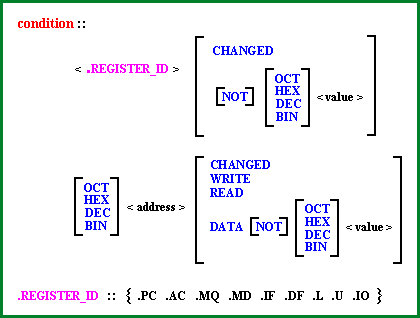
A trace trigger condition can be set on a specific register or an address, see the condition syntax.
An address in field #0 is 12 bit, but if the address is not in field #0, you can extend the address with the required
bits (field #1 needs one extra bit, field #4-7 need all three bits). All data entry is assumed in octal format
unless preceded by a data format keyword.
When the trigger condition is met, the simulator prints a dump of the registers after every executed instruction.
The check for the trigger condition is done after a pdp8 instruction is simulated.
The "register" .MD is the (just) executed pdp8 instruction as it is read from memory. The
".IO" is the simulation software collection of device interrupts flags (see the source code). As
there is not (yet) a bitmask AND / OR option, .IO traces will be tedious ...
The trace facility is not active by default, and the pdp8 simulator runs at best performance. When the simulator is
running pdp8 code and you suspect it is looping, hit ^T (Ctrl-T). The simulator will prompt for a trigger
specification, and from then on the trigger condition is checked after every simulated pdp8 instruction. It is clear this
will cause a drop of performance!
However, a situation can exist that you want to have the trace facility active with a trace specification defined right
from the start of the simulation of the pdp8 program.
Voil�, the command line switch "-t".
When you start the simulator with this switch, before anything else, the simulator will prompt for a trace
specification. Depending the trace specification, the simulator prints a dump of the registers right from the
start (with the UNTIL keyword) or start the output after the defined condition is met (with the
AFTER keyword). The ONLY keyword will produce output -as it says- only when the
condition is met.
For example, TRACE ONLY .MD 6211 will give a register dump only after every Change Data
Field (CDF) instruction to field #1.
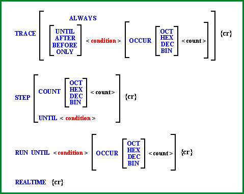
short description of the trace facility commands
- TRACE AFTER
- The pdp8 simulation will start in silent mode, no register dump is printed every instruction.
When the trace condition is met, the registers are printed after every executed pdp8 instruction.
With the "OCCUR" keyword you can specify how many times the condition must have been
met.
This keyword is available for all trace commands (except "TRACE ALWAYS").
- TRACE UNTIL
- A register dump is printed after every pdp8 instruction that is executed.
When the trace condition is met, the trace facility remains active (performance is low), but output is no longer printed.
With ^T (Ctrl-T) you can specify a new trace specification.
- TRACE BEFORE
- When the simulation runs, no output is printed, but the information is stored.
When the trace condition is met,
the last instruction information before the condition became true, is printed.
The amount of information stored
depends on the allocated size of the storage buffer, defined at assembly time.
The execution of the pdp8 code is stopped and a new trace specification is requested.
- TRACE ONLY
- A register dump is printed only after the pdp8 instruction that causes the condition to be met.
In the example (CDF #1), you can see fromn the trace output how often, and at which address(es) a change to data field #1
occurs.
- TRACE ALWAYS
- This is just an easy form to get a register dump after every executed pdp8 instruction.
You can follow the execution
of the code, but this method is faster than using the SINGLE STEP switch on the pdp8/e console.
- RUN UNTIL
- The trace facility is active, performance is so-so. The pdp8 code is executed without any trace output until the
condition is met. When the condition is met (and optionally the specified number of occurrences of the condition), a single
output line with the registers is printed.
The execution of the pdp8 code is stopped and a new trace specification is requested.
You must enter a new specification.
- STEP UNTIL
- This command has the same effect on the execution of the pdp8 code as the RUN UNTIL command.
However, the pdp8 code is executed -and- after every instruction the registers are printed until the
condition is met.
When the condition is met, the execution of the pdp8 code is stopped and a new trace specification is requested.
You must enter a new specification.
- STEP COUNT
- The trace facility is active and after every executed pdp8 instruction the registers are printed and the specified
count is decremented. When the count becomes zero a new trace specification is requested.
You must enter a new specification.
- REALTIME
- This is the option to disable the trace facility. The pdp8e simulator will run at a 100% performance figure.
The debugging of the trace facility goes well, so while at it, I added the "NOT" keyword, the
"BEFORE" option in the trace specification, all trace commands and the "RUN UNTIL"
command have an optional "OCCUR" keyword, and two new commands, "DISPLAY" and
"LOAD".
As "DISPLAY" and "LOAD" have nothing to do with tracing, I renamed the new stuff
"emulation commands", which include the trace facility :~).
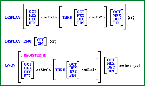 You can view the current pdp8/e registers and status, the contents of a single address (addrs1), specified in any data
format, displayed in any format.
You can view the current pdp8/e registers and status, the contents of a single address (addrs1), specified in any data
format, displayed in any format.
When you specify the "THRU" keyword, followed by a second address (addrs2), the contents of the
specified memory range is displayed. Of course, addrs2 must be higher than addrs1, but in the spirit of the pdp8 memory
design, you can not cross a field border, so both addrs1 and addrs2 are 12 bit, but you can add up to 3 more bits to
specify the field. In that case the bits [15:12] must be identical for both addresses.
With the "DISPLAY RF08" command you can enable/disable the printed output of the RF08 "registers"
just before the actual I/O (DMAR/DMAW) is executed. The default value at startup is
OFF.
The "LOAD" command enables you to change a pdp8/e register, a memory location, or fill a block of
consecutive memory locations with the specified data.
Some extra remarks on the emulation command entry line :
- as in CORESYS09, you can abbreviate the commands up till the initial letters are not ambiguous with other commands.
For example, "T A .PC 2345" is identical to
"TRACE AFTER .PC 2345" but then shorter :~) , only the letter "D"
displays the current registers/information line again.
- an other feature is ^Z (Ctrl-Z) when the emulation command prompt appears. Control-Z repeats the last entered command,
and you do not need to enter the <CR> to activate the command. This is very useful when you step
through the pdp8 code using for example "STEP COUNT 7"
(or "S C 7"). To step the next 7 instructions, just enter ^Z.
- the character input routine for emulation commands is also used by the pdp8 simulation (keyboard entry, but also
the low speed and high speed reader). This means that the data stream input to the pdp8 simulation can contain the
^T character. That would invoke the emulation command line. This kind of interference is not wanted, and the solution is
simple. If you do not start the pdp8 simulator with the command line switch "-t", the ^T character is accepted as on a
real pdp8. The disadvantage is when you want the emulation command prompt, but did not start the simulator with the "-t"
switch, you can not get to it. Note that the REALTIME command can be used to allow the simulation to run
at best performance, while keeping the option to invoke the emulation command prompt by entering ^T.
Just remember that any ^T will show this behaviour in this condition (reading a binary paper tape!).
As the total emulation command environment (including the trace facility) is just 2 kbytes of 6809 code, let me know
if you have other useful commands (or ideas) that you want to see included in the simulator.
Boot and run OS/8 (2nd try - debugging steps)
Alright. Armed with the emulation commands and the trace facility, I am confident that I can solve the problem of booting
OS/8.
The way I see it there are 3 stages, all executed in sequence and shown below.
- execution of the bootstrap code that gets the first block from the boot device
This piece of code is well-documented in the pdp8 handbooks. However, I re-wrote it so that the pdp8 code resembles
more the bootstrap code used to boot DMS. This code (just a few instructions) is *included* in the pdp8/e simulator
code. The OS/8 bootstrap code for DF32/RF08 disk is this (source: OS/8 System Generation Notes, table 7).
                  *7750
     7750  7600   0o7600        / CLA                      also Word Count !!
     7751  6603   DMAR          / read first block         also Current Address !!
     7752  6622   DFSC          / wait for I/O completion  also boot start address
     7753  5352   JMP    .-1
     7754  5752   JMP  I .-2
|
This is quite clever code, as the WORDCOUNT (o7750) and CURRENTADDRESS (o7751)
registers of the boot device are also the first 2 instructions! This bootstrap must be started from address o7750.
The CLA instruction also serves as WORDCOUNT, thus o0200 (128 decimal) words are
read from disk. The DMAR instruction also serves as CURRENTADDRESS, thus the
bootcode is loaded into memory from o6603 (locations o6603-o7003).
The "JMP .-1" instruction is the wait loop for read data transfer completion.
The "JMP I .-2" instruction jumps back to address o7752, where the contents (the
DFSC instruction) is used as the destination of the indirect jump address! So the start of
OS/8 is at o6622 - o6603 = o17 words offset from the address where the code is loaded.
To put the bootstrap code of DMS and OS/8 in a table inside the simulator software, I changed the OS/8 bootstrap code into
the "style" DMS bootcode looks. Then both bootstraps can be stored in a table which is selected by the command line switch
"-b". The WORDCOUNT register is loaded with o7600.
The CURRENTADDRESS register is loaded with o6603.
The OS/8 bootstrap becomes :
                  *adr          / any start address set by [SR]
     0000  7600   CLA           / AC := 0 --> disk (read) address
     0001  6603   DMAR          / read first block
     0002  6622   DFSC          / wait for I/O completion
     0003  5202   JMP    .-1
     0004  5605   JMP  I .+1
     0005  7600   6603          / execute loaded bootcode

     7750         *7750         / Data Break address start
     7750  7600   7600          / load Word Count
     7751  6622   6622          / load Current Address
|
To enable the bootstrap code to be loaded anywhere, the two JMP instructions must be relocated. This is done transparantly
by the simulator software. The command line switch "-bOS8" or
"-bDMS" enables the selection of the correct bootstrap when the SW switch
is raised and the LOAD ADDR switch is pushed the first time while the
HALT switch is active. At that moment the correct pdp8 bootstrap code is loaded into the pdp8 memory
space, at the address given by the Switch Register switches. This address is also loaded into the
PC register.
You start the execution of the bootstrap by de-activating HALT and pushing the CONT
switch. The bootstrap transfers control to the loaded code (device driver) from the boot device. If you specified the
command line switch "-v" (verbose), text is printed which OS is bootable from which address. Here is the output
from the simulator.
*EXEC 8300 -T -V -BOS8 -D1

  simulation command: STEP UNTIL .PC 6622


*** pdp8/e  SIMULATOR  v1.4 - 08aug2005 ***

PDP-8/e  12 kW core
  KM8-E  memory extension and timeshare control
  KE8-E  EAE (extended arithmetic element)
  KL8-E  Teletype keyboard/printer
  PC8-E  high-speed paper tape reader and punch
  RF08   Disk File, 4 RS08 disks -- ID=#1

[i] initialising pdp8/e core memory fields ... ok
[i] initialising Real Console hardware     ... ok
[i] initialising IDE hard disk interface   ... ok
    download binary file ->  end with ^Q   ... skipped

OS/8 bootstrap loaded at 5000
 Df=0 AC=0000 L=0 MQ=0000 U=0 ION=0 NoI=0 Ireq=00000
 If=0 In=7600 PC=5000 Df=0 AC=0000 L=0 MQ=0000 U=0 ION=0 NoI=0 Ireq=00000
 If=0 In=6603 PC=5001 Df=0 AC=0000 L=0 MQ=0000 U=0 ION=0 NoI=0 Ireq=00000
 If=0 In=6622 PC=5002 Df=0 AC=0000 L=0 MQ=0000 U=0 ION=0 NoI=0 Ireq=00000
 If=0 In=5202 PC=5003 Df=0 AC=0000 L=0 MQ=0000 U=0 ION=0 NoI=0 Ireq=00000
 If=0 In=6622 PC=5002 Df=0 AC=0000 L=0 MQ=0000 U=0 ION=0 NoI=0 Ireq=00000
 If=0 In=5605 PC=5004 Df=0 AC=0000 L=0 MQ=0000 U=0 ION=0 NoI=0 Ireq=00000
 If=0 In=1605 PC=6622

  simulation command: DISPLAY 6604 THRU 6646

               0       1       2       3       4       5       6       7
------------------------------------------------------------------------
006600                                    007000  006653  007647  007577
006610    000200  007605  007751  000000  000000  000000  000000  000000
006620    000000  000000  001605  006211  003606  006201  002205  002206
006630    005222  006643  006615  007600  001207  003612  001210  006603
006640    006623  005240  006621  007410  007402  005611  003344

  simulation command:
|
As you can see, the pdp8e simulator no longers starts at address $A300, but at $8300. I had to drop one field to add
the emulation command software in RAM (for testing). When all is fine it will be put in an EPROM, and field #3 becomes
available again for the pdp8e emulation memory space.
- execution of the device driver code that loads the first part of OS/8
In my case, the driver is the RF08SY system handler. This is
the listing of that driver,
and the data matches the previous "DISPLAY 6604 THRU 6646" command!
The loop at o6622-o6630 copies the data in field 0 into field 1.
The "RUN UNTIL" command of the trace facility comes in quite handy!
Then the next two blocks are read in from disk into field 0, starting at address o7577.
I must do an other test to see the WORDCOUNT value (07750). Also, reading
data from disk and storing the data in address o7600 will change WORDCOUNT
and CURRENTADDRESS in the process, if the initial WORDCOUNT
value higher than o0147 (in 2-complement). Again, here is the output from the simulator :
  simulation command: S C 12

 Df=0 AC=7607 L=0 MQ=0000 U=0 ION=0 NoI=0 Ireq=00000
 If=0 In=6211 PC=6623 Df=1 AC=7607 L=0 MQ=0000 U=0 ION=0 NoI=0 Ireq=00000
 If=0 In=3606 PC=6624 Df=1 AC=0000 L=0 MQ=0000 U=0 ION=0 NoI=0 Ireq=00000
 If=0 In=6201 PC=6625 Df=0 AC=0000 L=0 MQ=0000 U=0 ION=0 NoI=0 Ireq=00000
 If=0 In=2205 PC=6626 Df=0 AC=0000 L=0 MQ=0000 U=0 ION=0 NoI=0 Ireq=00000
 If=0 In=2206 PC=6627 Df=0 AC=0000 L=0 MQ=0000 U=0 ION=0 NoI=0 Ireq=00000
 If=0 In=5222 PC=6630 Df=0 AC=0000 L=0 MQ=0000 U=0 ION=0 NoI=0 Ireq=00000
 If=0 In=1605 PC=6622 Df=0 AC=7607 L=0 MQ=0000 U=0 ION=0 NoI=0 Ireq=00000
 If=0 In=6211 PC=6623 Df=1 AC=7607 L=0 MQ=0000 U=0 ION=0 NoI=0 Ireq=00000
 If=0 In=3606 PC=6624 Df=1 AC=0000 L=0 MQ=0000 U=0 ION=0 NoI=0 Ireq=00000
 If=0 In=6201 PC=6625

  simulation command: RU U .PC 6631

 Df=0 AC=0000 L=0 MQ=0000 U=0 ION=0 NoI=0 Ireq=00000
 If=0 In=6643 PC=6631

  simulation command: S U .PC 6636

 Df=0 AC=0000 L=0 MQ=0000 U=0 ION=0 NoI=0 Ireq=00000
 If=0 In=6615 PC=6632 Df=0 AC=0000 L=0 MQ=0000 U=0 ION=0 NoI=0 Ireq=00000
 If=0 In=7600 PC=6633 Df=0 AC=0000 L=0 MQ=0000 U=0 ION=0 NoI=0 Ireq=00000
 If=0 In=1207 PC=6634 Df=0 AC=7577 L=0 MQ=0000 U=0 ION=0 NoI=0 Ireq=00000
 If=0 In=3612 PC=6635 Df=0 AC=0000 L=0 MQ=0000 U=0 ION=0 NoI=0 Ireq=00000
 If=0 In=1210 PC=6636

  simulation command: D 7750 T 7751

               0       1       2       3       4       5       6       7
------------------------------------------------------------------------
007750    000000  007577

  simulation command: S U .PC 6645

 Df=0 AC=0200 L=0 MQ=0000 U=0 ION=0 NoI=0 Ireq=00000
 If=0 In=6603 PC=6637 Df=0 AC=0000 L=0 MQ=0000 U=0 ION=0 NoI=0 Ireq=00000
 If=0 In=6623 PC=6640 Df=0 AC=0000 L=0 MQ=0000 U=0 ION=0 NoI=0 Ireq=00000
 If=0 In=5240 PC=6641 Df=0 AC=0000 L=0 MQ=0000 U=0 ION=0 NoI=0 Ireq=00000
 If=0 In=6623 PC=6640 Df=0 AC=0000 L=0 MQ=0000 U=0 ION=0 NoI=0 Ireq=00000
 If=0 In=6621 PC=6642 Df=0 AC=0000 L=0 MQ=0000 U=0 ION=0 NoI=0 Ireq=00000
 If=0 In=7410 PC=6643 Df=0 AC=0000 L=0 MQ=0000 U=0 ION=0 NoI=0 Ireq=00000
 If=0 In=5611 PC=6645

  simulation command: D 6611

006611 in field number 0 [3E12] = 007605

  simulation command:
|
Stepping 10 instructions (remember, all numbers entered are default in the octal format!) shows that
the RF08SY system handler is entered. As the loop is a lot of instructions executed
(some 800...) I used the "RUN UNTIL" command to get quickly through the field copy
loop. Then stepping again to the end of RF08SY, and check that the indirect jump
address looks OK. It does! Remark: When the simulation stopped on a trace condition and you
enter a new command, you do not need to press the CONT switch to continue!
- execution of the "initial" OS/8 code that loads the rest of OS/8 in core
Click to see the
listing of OS/8 bootstrap code.
First, peek at some relevant memory locations, then step 7 instructions to verify that the OS/8
bootstrap code is started.
  simulation command: DISPLAY 7600 T 7615

               0       1       2       3       4       5       6       7
------------------------------------------------------------------------
007600    004207  005000  000000  000033  007602  006213  005267  000002
007610    007346  003304  001607  007004  007206  001305

  simulation command: DISPLAY 7665 T 7675

               0       1       2       3       4       5       6       7
------------------------------------------------------------------------
007660                                            006601  005607  000000
007670    000000  007330  002304  007610  005264  007346

  simulation command: STEP COUNT 7

 Df=0 AC=0000 L=0 MQ=0000 U=0 ION=0 NoI=0 Ireq=00000
 If=0 In=6213 PC=7605 Df=1 AC=0000 L=0 MQ=0000 U=0 ION=0 NoI=1 Ireq=00000
 If=0 In=5267 PC=7606 Df=1 AC=0000 L=0 MQ=0000 U=0 ION=0 NoI=0 Ireq=00000
 If=1 In=6202 PC=7667 Df=1 AC=0000 L=0 MQ=0000 U=0 ION=0 NoI=1 Ireq=00000
 If=1 In=4207 PC=7670 Df=1 AC=0000 L=0 MQ=0000 U=0 ION=0 NoI=0 Ireq=00000
 If=0 In=7346 PC=7610 Df=1 AC=7775 L=1 MQ=0000 U=0 ION=0 NoI=0 Ireq=00000
 If=0 In=3304 PC=7611 Df=1 AC=0000 L=1 MQ=0000 U=0 ION=0 NoI=0 Ireq=00000
 If=0 In=1607 PC=7612

  simulation command: STEP UNTIL .PC 7650

 Df=1 AC=0000 L=1 MQ=0000 U=0 ION=0 NoI=0 Ireq=00000
 If=0 In=7004 PC=7613 Df=1 AC=0001 L=0 MQ=0000 U=0 ION=0 NoI=0 Ireq=00000
 If=0 In=7206 PC=7614 Df=1 AC=0000 L=0 MQ=0000 U=0 ION=0 NoI=0 Ireq=00000
 If=0 In=1305 PC=7615 Df=1 AC=6603 L=0 MQ=0000 U=0 ION=0 NoI=0 Ireq=00000
 If=0 In=3251 PC=7616 Df=1 AC=0000 L=0 MQ=0000 U=0 ION=0 NoI=0 Ireq=00000
 If=0 In=1607 PC=7617 Df=1 AC=0000 L=0 MQ=0000 U=0 ION=0 NoI=0 Ireq=00000
 If=0 In=0306 PC=7620 Df=1 AC=0000 L=0 MQ=0000 U=0 ION=0 NoI=0 Ireq=00000
 If=0 In=3264 PC=7621 Df=1 AC=0000 L=0 MQ=0000 U=0 ION=0 NoI=0 Ireq=00000
 If=0 In=1607 PC=7622 Df=1 AC=0000 L=0 MQ=0000 U=0 ION=0 NoI=0 Ireq=00000
 If=0 In=7004 PC=7623 Df=1 AC=0000 L=0 MQ=0000 U=0 ION=0 NoI=0 Ireq=00000
 If=0 In=0236 PC=7624 Df=1 AC=0000 L=0 MQ=0000 U=0 ION=0 NoI=0 Ireq=00000
 If=0 In=7041 PC=7625 Df=1 AC=0000 L=1 MQ=0000 U=0 ION=0 NoI=0 Ireq=00000
 If=0 In=3350 PC=7626 Df=1 AC=0000 L=1 MQ=0000 U=0 ION=0 NoI=0 Ireq=00000
 If=0 In=7240 PC=7627 Df=1 AC=7777 L=1 MQ=0000 U=0 ION=0 NoI=0 Ireq=00000
 If=0 In=2207 PC=7630 Df=1 AC=7777 L=1 MQ=0000 U=0 ION=0 NoI=0 Ireq=00000
 If=0 In=1607 PC=7631 Df=1 AC=7777 L=1 MQ=0000 U=0 ION=0 NoI=0 Ireq=00000
 If=0 In=3351 PC=7632 Df=1 AC=0000 L=1 MQ=0000 U=0 ION=0 NoI=0 Ireq=00000
 If=0 In=2207 PC=7633 Df=1 AC=0000 L=1 MQ=0000 U=0 ION=0 NoI=0 Ireq=00000
 If=0 In=1264 PC=7634 Df=1 AC=0000 L=1 MQ=0000 U=0 ION=0 NoI=0 Ireq=00000
 If=0 In=6615 PC=7635 Df=1 AC=0000 L=1 MQ=0000 U=0 ION=0 NoI=0 Ireq=00000
 If=0 In=7600 PC=7636 Df=1 AC=0000 L=1 MQ=0000 U=0 ION=0 NoI=0 Ireq=00000
 If=0 In=1607 PC=7637 Df=1 AC=0000 L=1 MQ=0000 U=0 ION=0 NoI=0 Ireq=00000
 If=0 In=7012 PC=7640 Df=1 AC=2000 L=0 MQ=0000 U=0 ION=0 NoI=0 Ireq=00000
 If=0 In=7012 PC=7641 Df=1 AC=0400 L=0 MQ=0000 U=0 ION=0 NoI=0 Ireq=00000
 If=0 In=0310 PC=7642 Df=1 AC=0000 L=0 MQ=0000 U=0 ION=0 NoI=0 Ireq=00000
 If=0 In=6643 PC=7643 Df=1 AC=0000 L=0 MQ=0000 U=0 ION=0 NoI=0 Ireq=00000
 If=0 In=1607 PC=7644 Df=1 AC=0000 L=0 MQ=0000 U=0 ION=0 NoI=0 Ireq=00000
 If=0 In=7012 PC=7645 Df=1 AC=0000 L=0 MQ=0000 U=0 ION=0 NoI=0 Ireq=00000
 If=0 In=7012 PC=7646 Df=1 AC=0000 L=0 MQ=0000 U=0 ION=0 NoI=0 Ireq=00000
 If=0 In=7010 PC=7647 Df=1 AC=0000 L=0 MQ=0000 U=0 ION=0 NoI=0 Ireq=00000
 If=0 In=0307 PC=7650

  simulation command: DISPLAY 7750 T 7751

               0       1       2       3       4       5       6       7
------------------------------------------------------------------------
007750    000000  007777

  simulation command: STEP COUNT DEC 10

 Df=1 AC=0000 L=0 MQ=0000 U=0 ION=0 NoI=0 Ireq=00000
 If=0 In=6603 PC=7651 Df=1 AC=0000 L=0 MQ=0000 U=0 ION=0 NoI=0 Ireq=00000
 If=0 In=5664 PC=7652 Df=1 AC=0000 L=0 MQ=0000 U=0 ION=0 NoI=0 Ireq=00000
 If=0 In=7000 PC=0367 Df=1 AC=0000 L=0 MQ=0000 U=0 ION=0 NoI=0 Ireq=00000
 If=0 In=0035 PC=0370 Df=1 AC=0000 L=0 MQ=0000 U=0 ION=0 NoI=0 Ireq=00000
 If=0 In=7402 PC=0371
Program halt (HLT microcode in OPR instruction)
 Df=1 AC=0000 L=0 MQ=0000 U=0 ION=0 NoI=0 Ireq=00000
 If=0 In=7402 PC=0372


  simulation command: DISPLAY 7650 T 7717

               0       1       2       3       4       5       6       7
------------------------------------------------------------------------
007650    005613  006203  005664  000001  007346  003365  001624  007004
007660    007206  001366  003277  001624  000367  003313  001624  007004
007670    000264  007041  003211  007240  002224  001624  003212  002224
007700    006214  001254  003261  006201  001211  003775  001212  003774
007710    007402  001313  006615  007600  001624  007012  007012  000316

  simulation command:
|
Stepped the OS/8 bootstrap code until address 07650. As at address o7651 the
DMAR will read from the disk, I first checked
WORDCOUNT (o7750) and CURRENTADDRESS (o7751)
registers. As WORDCOUNT is o0000, 4096 words will be read,
and stored from address o0000 upward. Stepping a few instructions, shows that quite
some time elapses after the execution of the DMAR (o6603) and the
next instruction at o7652. In that period the LED of the CF Card flashes. The
indirect jump is the prelude to trouble ... the execution goes into the weeds and dies
in a HLT encountered at o0372.
The control-T of the trace facility returns control to me, so I can examine
the addresses at the end of the (SHNDLR) code.
The executed instruction at o7652 is NOT the
RDF instruction of the SHNDLR listing!
And again, Vince came up with the remark that pin-points the problem.
The Data Break facility of the pdp8 is actually what we call nowadays DMA. That means that
a real pdp8 can execute instructions while the data transfer from/to disk is in progress.
In fact, instruction execution proceeds, whenever the device is unable to present data in
the next cycle. OS/8 makes clever use of this, and executes instructions that will be
overwritten when the disk transfer (READ operation) is completed. The implementation of the
simulator (as it was) does the DMAR operation when the instruction is decoded,
and the next instruction is executed when the data transfer is completed. This scheme
overwrites the instructions that should have been executed before the transfer finishes.
OS/8 issues the DMAR, does some more instructions, and then checks the
device status, because it knows that the device cannot complete the READ in zero time.
To solve this deficiency in the "Data Break" facility, there are 2 possible implementations.
- "interleaved I/O"
After the IOT is executed, some mechanism "interleaves" the execution of the following pdp8
instructions. After every 8 (for example) instructions a small part of the I/O transfer is done.
This approach mimics the Data Break (DMA) quite accurate, but is difficult to implement.
- "deferred I/O"
When the I/O transfer IOT is executed, it only sets a global flag ("defer"), does the I/O
initialisation stuff (so that test IOTs like DFSC operate correct), and
sets a counter. After every following executed pdp8 instruction the count is decremented. When
the count reaches zero, the actual I/O transfer code is executed. When not any device has an
active count, the global "defer" flag is cleared.
As option #1 will make the code more complex, I went for option #2 (and coded it in one hour).
It requires a test and a branch instruction in the main pdp8 decode loop, but the performance
will stay the same, because a similar construction that implemented the physical latency delay
is no longer needed. Here is the output with the "deferred I/O" in the code, after the command
"RUN UNTIL .PC 7650".
  simulation command: D 7750 T 7751

               0       1       2       3       4       5       6       7
------------------------------------------------------------------------
007750    000000  007777

  simulation command: S C DEC 30

 Df=1 AC=0000 L=0 MQ=0000 U=0 ION=0 NoI=0 Ireq=00000
 If=0 In=6603 PC=7651 Df=1 AC=0000 L=0 MQ=0000 U=0 ION=0 NoI=0 Ireq=00000
 If=0 In=6214 PC=7652 Df=1 AC=0010 L=0 MQ=0000 U=0 ION=0 NoI=0 Ireq=00000
 If=0 In=1303 PC=7653 Df=1 AC=6212 L=0 MQ=0000 U=0 ION=0 NoI=0 Ireq=00000
 If=0 In=3264 PC=7654 Df=1 AC=0000 L=0 MQ=0000 U=0 ION=0 NoI=0 Ireq=00000
 If=0 In=6623 PC=7655 Df=1 AC=0000 L=0 MQ=0000 U=0 ION=0 NoI=0 Ireq=00000
 If=0 In=5255 PC=7656 Df=1 AC=0000 L=0 MQ=0000 U=0 ION=0 NoI=0 Ireq=00000
 If=0 In=6623 PC=7655 Df=1 AC=0000 L=0 MQ=0000 U=0 ION=0 NoI=0 Ireq=00000
 If=0 In=5255 PC=7656 Df=1 AC=0000 L=0 MQ=0000 U=0 ION=0 NoI=0 Ireq=00000
 If=0 In=6623 PC=7655 Df=1 AC=0000 L=0 MQ=0000 U=0 ION=0 NoI=0 Ireq=00000
 If=0 In=5255 PC=7656 Df=1 AC=0000 L=0 MQ=0000 U=0 ION=0 NoI=0 Ireq=00000
 If=0 In=6623 PC=7655 Df=1 AC=0000 L=0 MQ=0000 U=0 ION=0 NoI=0 Ireq=00000
 If=0 In=1624 PC=7656 Df=1 AC=0000 L=0 MQ=0000 U=0 ION=0 NoI=0 Ireq=00000
 If=0 In=7004 PC=7657 Df=1 AC=0000 L=0 MQ=0000 U=0 ION=0 NoI=0 Ireq=00000
 If=0 In=7206 PC=7660 Df=1 AC=0000 L=0 MQ=0000 U=0 ION=0 NoI=0 Ireq=00000
 If=0 In=1366 PC=7661 Df=1 AC=0300 L=0 MQ=0000 U=0 ION=0 NoI=0 Ireq=00000
 If=0 In=3277 PC=7662 Df=1 AC=0000 L=0 MQ=0000 U=0 ION=0 NoI=0 Ireq=00000
 If=0 In=1624 PC=7663 Df=1 AC=0000 L=0 MQ=0000 U=0 ION=0 NoI=0 Ireq=00000
 If=0 In=0367 PC=7664 Df=1 AC=0000 L=0 MQ=0000 U=0 ION=0 NoI=0 Ireq=00000
 If=0 In=3313 PC=7665 Df=1 AC=0000 L=0 MQ=0000 U=0 ION=0 NoI=0 Ireq=00000
 If=0 In=1624 PC=7666 Df=1 AC=0000 L=0 MQ=0000 U=0 ION=0 NoI=0 Ireq=00000
 If=0 In=7004 PC=7667 Df=1 AC=0000 L=0 MQ=0000 U=0 ION=0 NoI=0 Ireq=00000
 If=0 In=0264 PC=7670 Df=1 AC=0000 L=0 MQ=0000 U=0 ION=0 NoI=0 Ireq=00000
 If=0 In=7041 PC=7671 Df=1 AC=0000 L=1 MQ=0000 U=0 ION=0 NoI=0 Ireq=00000
 If=0 In=3211 PC=7672 Df=1 AC=0000 L=1 MQ=0000 U=0 ION=0 NoI=0 Ireq=00000
 If=0 In=7240 PC=7673 Df=1 AC=7777 L=1 MQ=0000 U=0 ION=0 NoI=0 Ireq=00000
 If=0 In=2224 PC=7674 Df=1 AC=7777 L=1 MQ=0000 U=0 ION=0 NoI=0 Ireq=00000
 If=0 In=1624 PC=7675 Df=1 AC=7777 L=1 MQ=0000 U=0 ION=0 NoI=0 Ireq=00000
 If=0 In=3212 PC=7676 Df=1 AC=0000 L=1 MQ=0000 U=0 ION=0 NoI=0 Ireq=00000
 If=0 In=0300 PC=7677 Df=1 AC=0000 L=1 MQ=0000 U=0 ION=0 NoI=0 Ireq=00000
 If=0 In=6214 PC=7700

  simulation command: S C DEC 20

 Df=1 AC=0010 L=1 MQ=0000 U=0 ION=0 NoI=0 Ireq=00000
 If=0 In=1254 PC=7701 Df=1 AC=7356 L=1 MQ=0000 U=0 ION=0 NoI=0 Ireq=00000
 If=0 In=3261 PC=7702 Df=1 AC=0000 L=1 MQ=0000 U=0 ION=0 NoI=0 Ireq=00000
 If=0 In=6201 PC=7703 Df=0 AC=0000 L=1 MQ=0000 U=0 ION=0 NoI=0 Ireq=00000
 If=0 In=1211 PC=7704 Df=0 AC=0000 L=1 MQ=0000 U=0 ION=0 NoI=0 Ireq=00000
 If=0 In=3775 PC=7705 Df=0 AC=0000 L=1 MQ=0000 U=0 ION=0 NoI=0 Ireq=00000
 If=0 In=1212 PC=7706 Df=0 AC=7777 L=1 MQ=0000 U=0 ION=0 NoI=0 Ireq=00000
 If=0 In=3774 PC=7707 Df=0 AC=0000 L=1 MQ=0000 U=0 ION=0 NoI=0 Ireq=00000
 If=0 In=7402 PC=7710
Program halt (HLT microcode in OPR instruction)
 Df=0 AC=0000 L=1 MQ=0000 U=0 ION=0 NoI=0 Ireq=00000
 If=0 In=7402 PC=7711


 D 7650 T 7737

               0       1       2       3       4       5       6       7
------------------------------------------------------------------------
007650    005613  006203  005664  000001  007346  003365  001624  007004
007660    007206  007356  003277  001624  000367  003313  001624  007004
007670    000264  007041  003211  007240  002224  001624  003212  000300
007700    006214  001254  003261  006201  001211  003775  001212  003774
007710    007402  001313  006615  000000  001624  007012  007012  000316
007720    006643  001624  007012  007012  007010  000370  007402  006214
007730    001222  003313  006623  005303  004213  002224  006621  007410

  simulation command:
|
Of course, we first look how it ends. Bummer, still a HALT occurs. However, the
RDF instruction at o7652 is executed, as are some following
instructions. At o7655-o7656 the test-and-wait for I/O completion loop is executed.
I initialized the "deferred I/O counter" to 10, and that works nicely. The initial
count value of 10 is just a value, a better number is to be determined, if needed.
Note that the ISZ instruction at o7657 in the listing is not
executed as it is overwritten with the read-in 4k data! Also, the last time the
wait loop is executed, the JMP .-1 instruction at o7656 is
replaced by a TAD instruction (o1624).
I took a look at SIMH pdp8, and entered the commands "br 7650" and then "boot rf".
When the breakpoint occurs I entered "e 7650-6777" and it matches the SHNDLR listing.
I 's'tepped further one by one. The DMAR occurs, then the RDF, TAD and DCA which deposit
"CIF 1" in location SFIELD. I wondered "why deposit that there, it will be overwritten".
Stepping further gives the following flow (PC - instruction):
     7655 - DISK
     7656 - JMP  7655
here is the wait for I/O completion loop. I entered "br 7657" and "cont". The breakpoint
occurs, and "e 7657-7677" (in SIMH) shows that the memory is NOT overwritten! o7664 still
contains o6212 (CIF 1). Stepping again one instruction at a time:
     7660 - DFSE
     7661 - SKP
     7663 - ISZ  7607
     7664 - CIF  1
     7665 - DCMA
     7666 - JMP  I 7607
    17675 - CIF CDF 0      * note: in field 1
    17676 - JMP  I 7677    *
     0400 - JMP  I 505
     1005 - CDF  1
and so on, but that is not relevant at this time.
I started the SIMH pdp8 again and just for the DMAR (breakpoint at o7650) I checked o7750
and o7751. They are o6000 (!!!) and o7777.
Conclusion: the simulator sets the WordCount incorrect! At some point AC must have
the value o6000 which will be deposited in o7750 with an DCA instruction. So, I stepped the
simulator and SIMH simultaneous both one instruction at a time and followed the contents of AC.
They are different too!
At address 6645, the JMP I B7605 goes to o7605. There is a CIF CDF 1, and then a JMP to o7667
(in field 1!) because of the previous CIF CDF. In field 1 at o7667 are the following instructions:
   (1) 7667  6202  CIF  0
   (1) 7670  4207  JMS  7606
Before the JMS, the contents of o7607 is o0002 (see the output screen above, both in the simulator
and in SIMH). After the JMS the PC becomes o7610, DF=1 and IF=0. However, in SIMH the location o7607
(in field 0) contains o7671, and in the simulator it is still o0002, but the value o7671 is stored
in field 1 at o7607! So, SIMH does first the I field change, then stores the return address,
where the simulator first stores the return address and then changes the I field! Here is a piece the
output.
 Df=1 AC=0000 L=0 MQ=0000 U=0 ION=0 NoI=0 Ireq=20000
 If=1 In=6202 PC=7667

  simulation command: S C 1

 Df=1 AC=0000 L=0 MQ=0000 U=0 ION=0 NoI=1 Ireq=20000
 If=1 In=4207 PC=7670

  simulation command: D 7607

007607 in field number 0 [420E] = 000002

  simulation command: S C 1

 Df=1 AC=0000 L=0 MQ=0000 U=0 ION=0 NoI=0 Ireq=20000
 If=0 In=7346 PC=7610

  simulation command: D 7607

007607 in field number 0 [420E] = 000002

  simulation command: S C 1

 Df=1 AC=7775 L=1 MQ=0000 U=0 ION=0 NoI=0 Ireq=20000
 If=0 In=3304 PC=7611

  simulation command: D 7607

007607 in field number 0 [420E] = 000002

  simulation command: D 17607

007607 in field number 1 [620E] = 007671

  simulation command: LOAD 7607 7671

  simulation command: D 7607

007607 in field number 0 [420E] = 007671

  simulation command: S C 7

 Df=1 AC=0000 L=1 MQ=0000 U=0 ION=0 NoI=0 Ireq=20000
 If=0 In=1607 PC=7612 Df=1 AC=1000 L=1 MQ=0000 U=0 ION=0 NoI=0 Ireq=20000
 If=0 In=7004 PC=7613 Df=1 AC=2001 L=0 MQ=0000 U=0 ION=0 NoI=0 Ireq=20000
 If=0 In=7206 PC=7614 Df=1 AC=0000 L=0 MQ=0000 U=0 ION=0 NoI=0 Ireq=20000
 If=0 In=1305 PC=7615 Df=1 AC=6603 L=0 MQ=0000 U=0 ION=0 NoI=0 Ireq=20000
 If=0 In=3251 PC=7616 Df=1 AC=0000 L=0 MQ=0000 U=0 ION=0 NoI=0 Ireq=20000
 If=0 In=1607 PC=7617 Df=1 AC=1000 L=0 MQ=0000 U=0 ION=0 NoI=0 Ireq=20000
 If=0 In=0306 PC=7620

  simulation command: R

.dir

No memory allocated for this field
 Df=1 AC=0000 L=1 MQ=0000 U=0 ION=0 NoI=0 Ireq=20000
 If=0 In=6623 PC=7655
|
As you see, I used the "LOAD" command to patch o7607 in field 0.
When I step the code, I now also see values in AC that correspond with the ones I
see in SIMH. That was neither the case before the "patch". I got bold: entered the
"R" command (realtime).
***** I get the OS/8 dot prompt! *****
Then I entered "DIR", but it fails. But the dot was making me happy :-)
I changed the sequence in the JMS code to first check for an I field change and then
store the correct return address. Ran the simulator again with a breakpoint at o7610
to see if the corrected JMS code works ...
OS/8 bootstrap loaded at 5000
 Df=1 AC=0000 L=0 MQ=0000 U=0 ION=0 NoI=0 Ireq=00000
 If=0 In=7346 PC=7610

  simulation command: D 7607

007607 in field number 0 [420E] = 007671

  simulation command: R

.dir
SYSTEM ERR
.
|
After the "dir" command I get "SYSTEM ERR", but that might be logical because I read in only
the A0.S19 file, and not all the others ... Notice, it recovers and I get the dot prompt back!
After I loaded some 10 additional .S19 files, I still get "SYSTEM ERR". Vince took an other
look at the JMSsub code, found one more error, and came up with the correction!
*EXEC 8300 -V -BOS8 -D1

*** pdp8/e  SIMULATOR  v1.5 - 24aug2005 ***

PDP-8/e  12 kW core
  KM8-E  memory extension and timeshare control
  KE8-E  EAE (extended arithmetic element)
  KL8-E  Teletype keyboard/printer
  PC8-E  high-speed paper tape reader and punch
  RF08   Disk File, 4 RS08 disks -- ID=#1

[i] initialising pdp8/e core memory fields ... ok
[i] initialising Real Console hardware     ... ok
[i] initialising IDE hard disk interface   ... ok
    download binary file ->  end with ^Q   ... skipped

OS/8 bootstrap loaded at 5000

.VERSION
OS/8 - KBM V3Q - CCL V1F

.BASIC
NEW OR OLD--OLD SPACWR.BA

READY
RUN

SPACWR  BA    5A

                  * * *  STAR TREK  * * *


        FOR INSTRUCTIONS USE OS-8 HELP COMMAND FOR 'SPACWR'


YOU MUST DESTROY 12 KLINGONS IN 30 STARDATES WITH 1 STARBASES

------------------------

          *     *                       STARDATE         3900
 *                                      CONDITION        GREEN
                                        QUADRANT         5 , 3
    *                                   SECTOR           8 , 2
                                        TOTAL ENERGY     3000
                                        PHOTON TORPEDOES 10
   <*>    *        *  *                 SHIELDS          0
------------------------

COMMAND:?2

LONG RANGE SENSOR SCAN FOR QUADRANT 5 , 3
-------------------
: 2   : 7   : 4   :
-------------------
: 6   : 7   : 8   :
-------------------
: 8   : 8   : 1   :
-------------------
COMMAND:?
|
This looks very good, but what you can not see is how long it took.
How about more than 15 minutes before I could enter RUN and another some
5 minutes before I could enter my first command? Time to upgrade the Core board to 2 MHz!
Get the simulator software
Click here to get the latest version (95 kbyte) with all
corrections up till now, including the emulation & trace facility code (and bugs ...?!).
Loose ends to work on:
- Why does the LOADER inside DMS seem to load the .BIN papertape, but after saving the data to disk, and
then starting the file from disk it runs into a HLT instruction.
... to be continued ...
Performance of the simulator
I already told that this simulator is not a speed devil. Now that some debugging is finished I can run
the DIGITAL diagnostics which give an indication of its execution time and compare that to the time that
the simulator needs ...
Diagnostic
|
Execution time on real PDP-8
(according the diagnostic listing) |
Simulator execution |
| 6809 at 1 MHz | 6809 at 2 MHz |
| MAINDEC-8E-D0AB | approx. 5 sec for 1440 passes |
10 min : 47 sec | 5 min : 19 sec |
| MAINDEC-8E-D0BB | approx. 5 sec for 1550 passes |
9 min : 52 sec | 4 min : 51 sec |
On average you could say that the real PDP-8 is approximately 120 times faster than this 6809-based simulator
running at 1 MHz! After the 6809 clock is doubled by changing the Motorola 6809/6850/6821 to their "B" parts, and
removing the 4 MHz / installing an 8 MHz Xtal oscillator, the figures get better by a factor 2 (as expected
).
Note that the RAM chips and the EPROM must have an access time below 250 ns to run the Core Board at 2 MHz.
However, the speed compared to a real PDP-8 depends on the mix of instructions. The listing of the
(MAINDEC-8E-DHMCA) Extended Memory diagnostic says that the full test for all 8 fields runs
approximately for 3:40 minutes. Extrapolation with a factor ~120 would mean that the simulator will need over 7 hours
to complete the full test. Since the simulator has only 4 fields (maximum possible, given the Core Board design), it
turns out that the full test for 4 fields "only" takes 1 hour and 50 minutes.
I can not check that 8 fields would indeed run for over 7 hours!
Compatibility with a real pdp8/e
The following diagnostic and application programs have been tested in this pdp8/e simulator.
The mentioned execution times are measured when the 6809 clock was running at 1 MHz, unless an explicit
remark (2 MHz) is written after the execution time.
| diagnostic program |
runs OK ? |
description / remarks |
|---|
| MAINDEC-8E-D0AB-PB |
yes |
pdp-8/e instruction test part #1
start with PC=0200 / SR=7777.
The test halts at 0147 with AC=0000. CONT.
Every 11 minutes the test outputs a BELL character |
| MAINDEC-8E-D0BB-PB |
yes |
pdp-8/e instruction test part #2
start with PC=0200.
Every 10 minutes the test outputs a BELL character |
| MAINDEC-8E-D0DB-PB |
yes |
random AND test
start with PC=0200.
Every 4 minutes the test prints "A" |
| MAINDEC-8E-D0EB-PB |
yes |
random TAD test
start with PC=0200.
Every 10 minutes the test prints "T" |
| MAINDEC-8E-D0FC-PB |
yes |
random ISZ test
start with PC=0200.
Every 12 minutes the test prints "FC" |
| MAINDEC-8E-D0GC-PB |
yes |
random DCA test
start with PC=0200.
Every 8 minutes the test outputs a BELL character |
| MAINDEC-8E-D0HC-PB |
yes |
random JMP test
start with PC=0200.
Every 14 minutes the test prints "HC" |
| MAINDEC-8E-D0IB-PB |
yes |
basic JMP-JMS test
start with PC=0200.
Every 13 minutes the test outputs a BELL character |
| MAINDEC-8E-D0JC-PB |
yes |
random JMP-JMS test
start with PC=0200.
Every 16 minutes the test prints "JC" |
| MAINDEC-08-DHMCA-A-PB |
yes |
pdp-8/e memory extension & time share control test
start with PC=0200 / SR0=0 and SR9-SR10-SR11='010'.
The test checks 3 fields. Every 73 minutes (!) the test outputs a BELL character |
| MAINDEC-08-DHKMA-A-PB |
yes |
pdp-8/e extended memory data & checkerboard test
start with PC=0200 / SR5=1, SR06:SR8='001',
SR09:SR11='001' (test field 1).
The test checks 1 field. Every 10.5 minutes the test completes (set by SR05)
|
| MAINDEC-8E-D1FB-PB |
tbt |
pdp-8/e extended memory address test (EA8E) |
| application program |
runs OK ? |
description / remarks |
|---|
| DEC-P8-SBAF-PB |
yes |
Disk Monitor System (DMS) Builder
start with PC=0200. |
| MAINDEC-08-D5DB-PB |
yes |
DF32 multi disk diagnostic test
This is not a diagnostic, but more a confidence test. |
| DEC-S8-ODRFA-B-PB |
tbt |
0056.pt/0138.pt RF08 CONFIG. V6 |
| DEC-S8-ODDFA-B-PB |
tbt |
0058.pt/0139.pt DF32 CONFIG. V6 |
| FOCAL '68 |
tbt |
0060.pt start address 200 (press continue twice) |
| DEC-08-AJAE-PD |
tbt |
0062.pt FOCAL, 1969 + INIT 4K INIT |
| FOCAL '71 |
tbt |
0059.pt start address 200 (press continue once) |
tbt :: to be tested (because no test description / documentation is available)
... to be continued ...
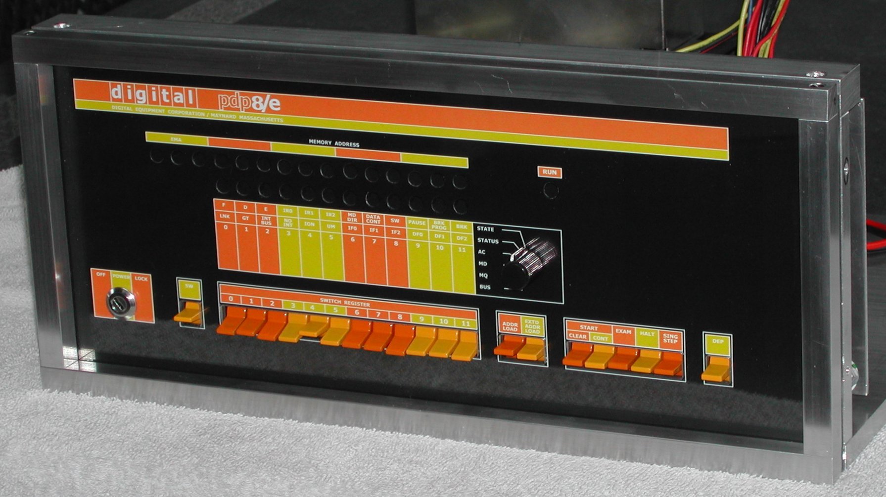