
with the location of the jumpers/switches,
click on the image of the module.
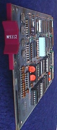
| 11/34A MR11-EA | M9312 |
| - Bootstrap / terminator |
| Quick jumps within this page | |
|---|---|
|
|
|
|
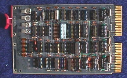
To see a larger image (size is 80414 bytes) with the location of the jumpers/switches, click on the image of the module. |
General description of the M9312
The M9312 Bootstrap/terminator module contains a complete set of UNIBUS termination resistors and 512 words of ROM that can be used for diagnostic routines, the console emulation routine and bootstrap programs. The module has 12 jumpers, W1 thu W12, and five sockets to put ROM's in. One socket is used for a diagnostic ROM for the PDP-11/60 or PDP-11/70, or for a ROM that contains the console emulation routine and diagnostics for all other PDP-11's. The other four sockets accept ROM's that contain bootstrap programs.
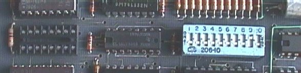
Diagnostics, bootstrap programs and the console emulator routine are all selectable through the DIP switches
on the M9312. The switch settings and addresses depend on the particular socket the ROM's are placed in.
M9312 routines may be initiated in the following ways:
| Back to top |
Of course, system power should be turned off ....
 |
|
| Back to top |
Automatic booting on power-up can be enbled with DIP switch S1-2. When this
switch is set to the OFF position the processor will execute its power-up routine normally, obtaining the
PC from location 24(8) and the PSW from location 26(8). When the switch is in the ON position during power-up
the processor will obtain its PC and PSW from the locations 773024(8) and 773026(8). The address of the DIP
switches S1-1 and S1-3 thru S1-10 is 773024(8).
The function of the power-up boot enable switch S1-2 can be duplicated by an external switch connected to
the faston tabs TP3 and TP4. A closed switch connected to TP3 and TP4 is equivalent to S1-2 set to ON.
When MOS memory is present with battery backup, a battery status signal is generated by the power supply.
This signal should be connected to the power-up boot enable input (TP4). When TP4 is used, DIP switch S1-2
must be OFF.
The faston tabs TP1 thru TP4 are near the handle of the module with TP1 nearest to the edge
of the PCB.
TP1 - boot signal input
TP2 - boot signal return
TP3 - power-up
boot enable return
TP4 - power-up boot enable input
| Back to top |
| W1 | connects pull up for BUS BG6 H (when IN) |
| W2 | connects pull up for BUS BG7 H (when IN) |
| W3 | connects pull up for BUS NPG H (when IN) |
| W4 | connects pull up for BUS BG5 H (when IN) |
| W5 | connects pull up for BUS BG4 H (when IN) |
| W6 | connect BUF VECTOR L to finger BD1 (IN for PDP-11/70) |
| W7 | reserved (always IN) |
| W8 | connects LO ROM ENABLE H (when OUT) |
| W9, W10 | install for power-up boot to 773024(8) (IN for all CPU's except 11/60) |
| W11, W12 | install for power-up boot to 773224(8) (IN for PDP-11/60 only) |
| Back to top |
Console emulator & diagnostics
Socket E20 is reserved for the diagnostics and console emulator ROM.
| Diagnostic | Start address | S1 switch settings for power-up or push-button boot | |||||||||
|---|---|---|---|---|---|---|---|---|---|---|---|
| 1 | 2 | 3 | 4 | 5 | 6 | 7 | 8 | 9 | 10 | ||
| no | 165144 | ON | * | OFF | OFF | ON | ON | OFF | OFF | ON | OFF |
| yes | 165020 | ON | * | OFF | OFF | OFF | OFF | ON | OFF | OFF | OFF |
The start address can be loaded, and the program can be started from a programmer's console or switch register,
if a power-up start
or external boot start from the M9312 is not used.
If you want a description of the commands of the console emulator, send me an e-mail.
I will add a link here.
 | ||||||||||||
| S1 switch | 1 | 3 | 4 | 5 | 6 | 7 | 8 | 9 | 10 | (*) | ||
|---|---|---|---|---|---|---|---|---|---|---|---|---|
| corresponding bus address bits | 12 | 11 | 10 | 8 | 7 | 6 | 5 | 4 | 3 | 2 | 1 | 0 |
| binary value of switches | x | x | x | x | x | x | x | x | 0 | |||
| octal value of switches | X | Y | Z | |||||||||
* No switch is provided for setting bit 0.
Therefore only an even address (for the PC) can be set.
Bootstrap ROM's
| part number | device | mnemonic | unit | CSR |
|---|---|---|---|---|
| 23-751A9 | RL01 | DL | 0-3 | 774400 |
| 23-752A9 | RK06/07 | DM | 0-7 | 777440 |
| 23-753A9 | RX01 | DX | 0-1 | 777170 |
| 23-755A9 | RP02/03 | DP | 0-7 | 776714 |
| RP04/05/06 RM02/03 | DB | 0-7 | 776700 | |
| 23-756A9 | RK03/05/05J | DK | 0-7 | 777404 |
| TU55/56 | DT | 0-7 | 777342 | |
| 23-757A9 | TU16 | MM | 0-7 | 772440 |
| 23-758A9 | TU10 TS03 | MT | 0-7 | 772522 |
| 23-759A9 | RS03/04 | DS | 0-7 | 772040 |
| 23-760A9 | PC05 | PR | n/a | 777550 |
| LO SPD RDR | TT | n/a | 777560 | |
| 23-761A9 | TU60 | CT | 0-1 | 777550 |
| 23-764A9 | TS04 | MS | 0-3 | 772520 |
| 23-765A9 | TU58 | DD | 0-1 | 776500 |
| 811A9 | RX02 | DY | 0-1 | 777170 |
When you click on the part number, a window opens with the DIP switch settings
that apply for the ROM.
As the DIP switches set the bootstrap routine start address, the settings differ when the ROM is
placed in an other socket.
| Back to top |
The only documentation I have is the "M9312 bootstrap/terminator module technical manual", EK-M9312-TM-002.
Important to know is that the module draws typical 1.5 Amps from the +5 Volt power supply. This is important because the M9312
must be in the backplane that holds the processor boards as well. When you install the floating point processor and the
cache memory option, you must do some power calculations to make sure that you do not overload the +5 Volt power supply.
Also note that the four boot ROM sockets are NOT in the 'normal' order, that is 1-2-3-4. Starting from the edge of the board
where the handle is, and going toward the backplane contacts, the order is ROM #1, ROM #3, ROM #2 and finally ROM #4.
Other documentation.
| Back to top |